opt_ex15 : Three Terminal R3_CMC Resistor Model Extraction
Requires: Utmost IV, SmartSpice, SmartView
Minimum Versions: Utmost IV 1.11.0.R, SmartSpice 4.10.2.R, SmartView 2.28.2.R
This example describes how to extract a three terminal r3_cmc model including temperature coefficients and parasitic parameters. This model is designed to model lightly doped resistors, such as well resistors and in this case we will model an nwell resistor.
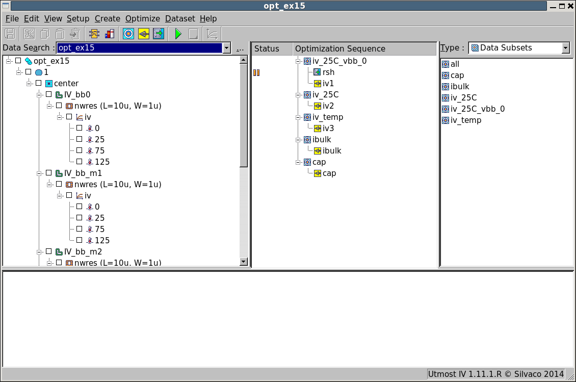
The project file opt_ex15.prj and the data file opt_ex15.uds for this example should both be loaded into your database. When opened, the project will look as shown in opt_ex15_01.png .
There are five sections in the extraction sequence. The first three sections deal with the main resistor at room temperature, with back bias and then with temperature effect. The last two sections deal with the parasitic diode current and capacitance to the third terminal. The objective of each section is to isolate a device characteristic and then to extract or optimize only those model parameters which account for this device effect.
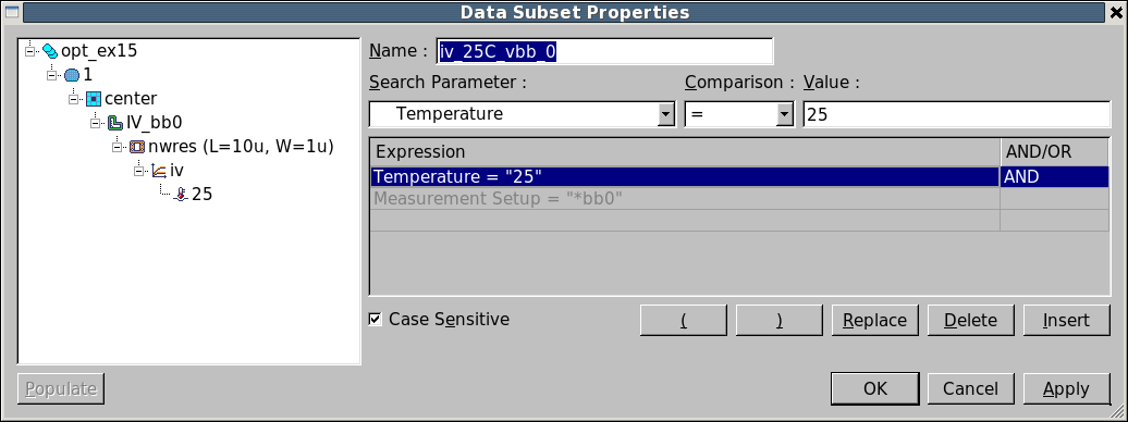
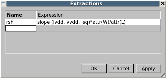
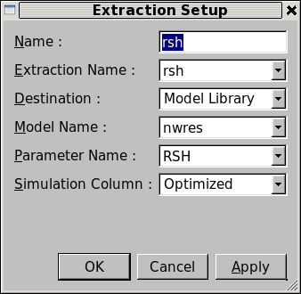
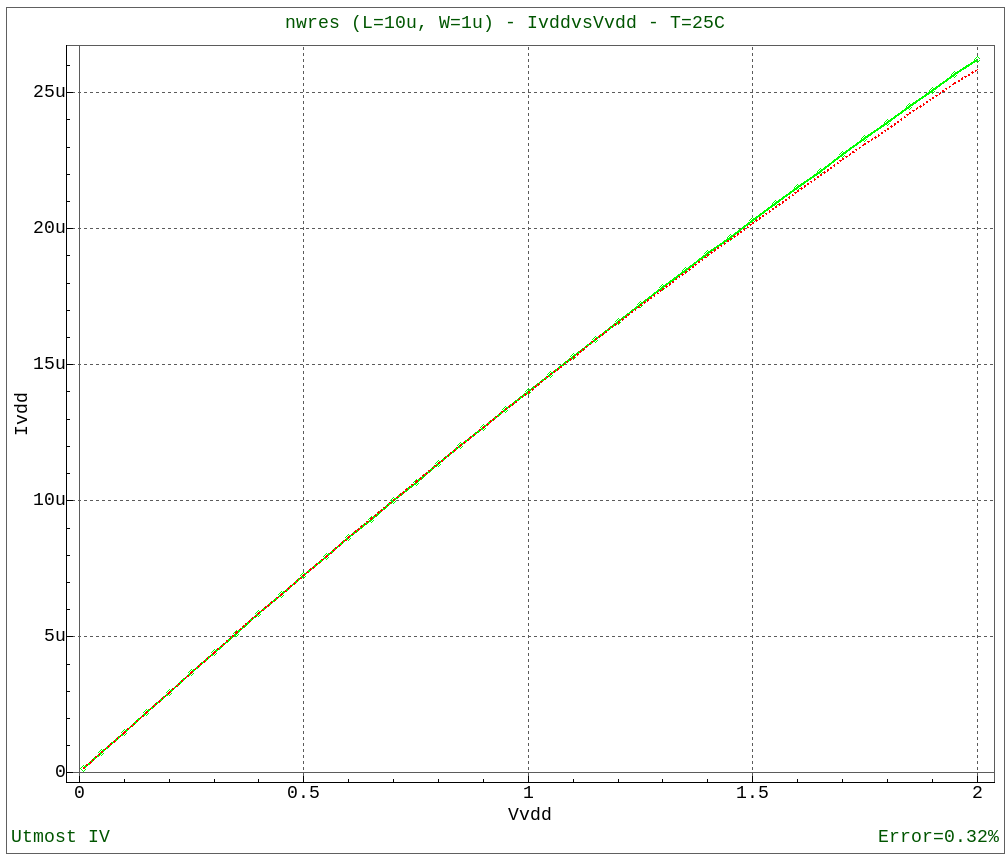
The first section, selects the resistor measurement at the nominal temperature, as shown in opt_ex15_02.png . From this single dataset, we pre-extract a sheet resistance value. This is done by the extraction 'rsh' which is defined as shown in opt_ex15_03.png . The extraction setup, also called 'rsh', is used to select the extraction to be performed on the single dataset and also defines where to write the result as shown in opt_ex15_04.png . In this case, the extraction called 'rsh' is performed and the result is written into the model parameter RSH of the model NWRES into the optimized column. Then we optimize the sheet resistance parameter again along with parameters describing the velocity saturation of the device. Once this optimization has been run, the measured vs simulated IV characteristics are displayed in the viewer as shown in opt_ex15_05.png .
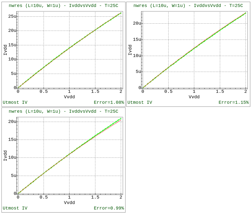
The second section deals with the change in the resistance due to the bias effect from the third terminal. For an nwell resistor, with a pbulk region, negative bias on the ptype third terminal will reverse bias the junction and extend a depletion region into the nwell which will pinch off the resistor. This will increase the resistivity of the nwell resistor layer. For this optimization we will use datasets at the nominal temperature, but with differing back biases. Once this optimization has been run, the measured vs simulated characteristics are displayed in the viewer as shown in opt_ex15_06.png .
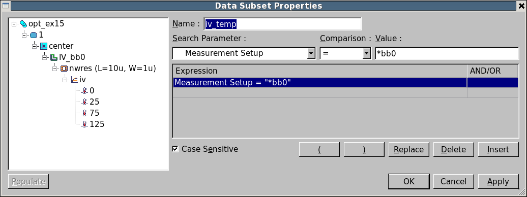
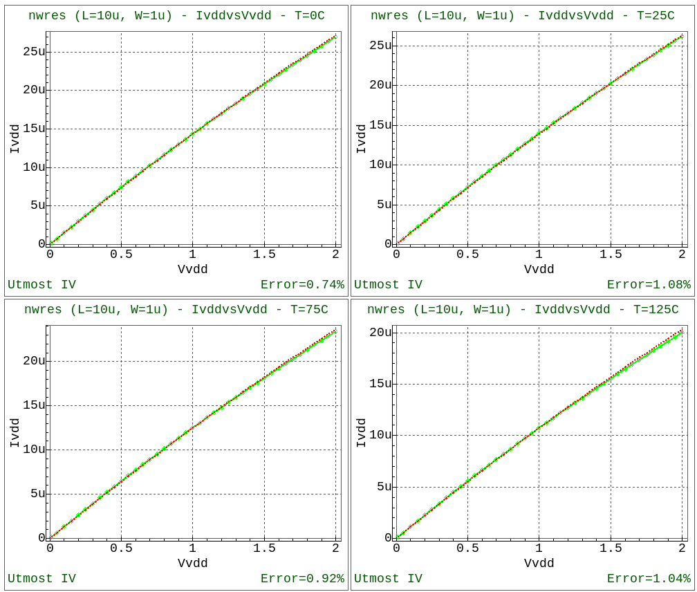
The third section deals with the temperature coefficients. One resistor has been measured at four temperatures and the dataset subset definition is as shown in opt_ex15_07.png . The first and second order temperature coefficients TC1 and TC2 are optimized. Once this optimization has been run, the measured vs simulated IV and extracted characteristics are displayed in the viewer as shown in opt_ex15_08.png .
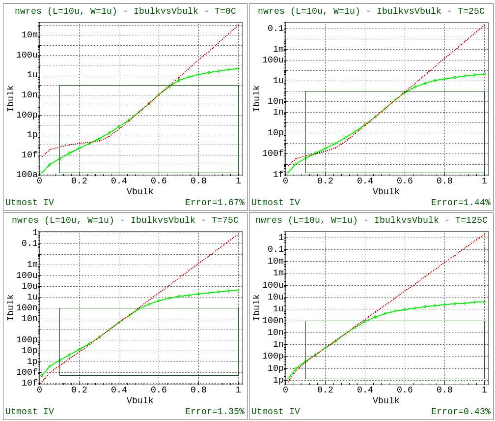
The fourth section deals with the forward diode parasitic current optimization. Note that the model does not account for the roll off in current with higher forward biases, however, it is not intended that this junction be forward biased during normal resistor operation. After optimization the measured vs modeled parasitic current characteristics are as shown in opt_ex15_09.png .
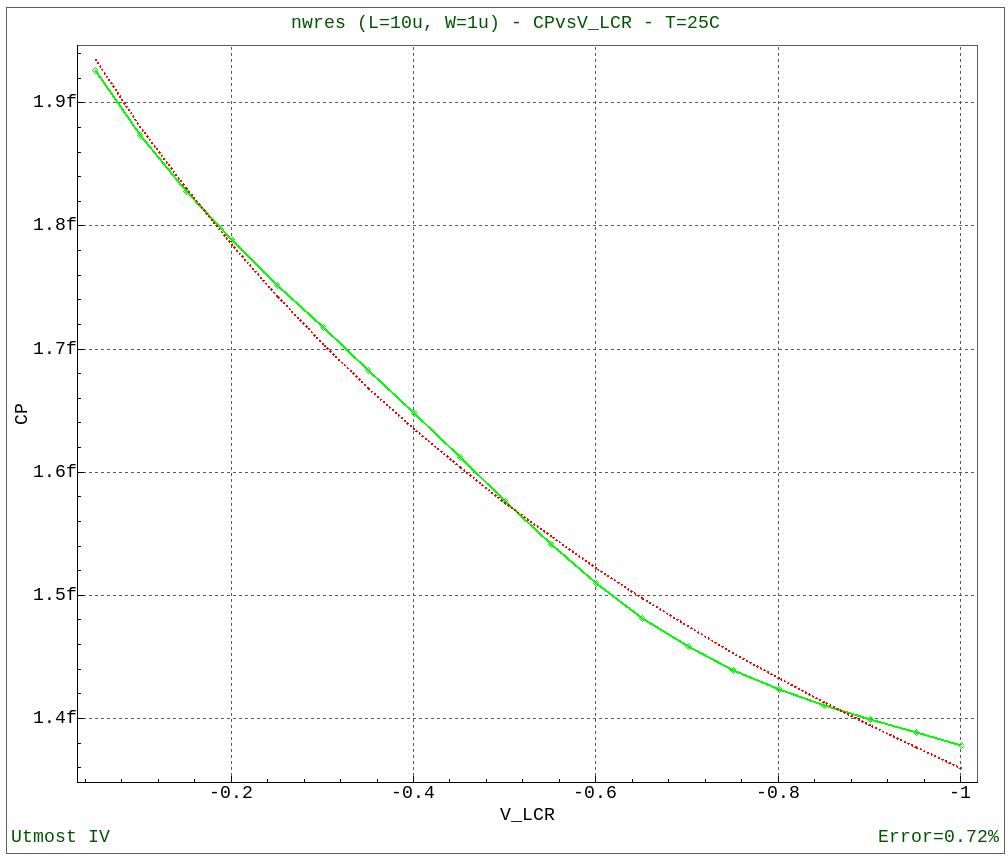
Finally in the fifth section, the parasitic reverse junction capacitance of the n-well resistor to the p bulk is optimized. After optimization the measured vs modeled characteristic will be as shown in opt_ex15_10.png .
The model card can then be exported into an external model library file as shown in the output file opt_ex15.lib.
opt_ex15.lib
											.MODEL nwres R3_CMC (
+LEVEL    = 1003           VERSION  = 1
+SUBVERSION = 0
+REVISION = 0              TYPE     = -1             SCALE    = 1
+SHRINK   = 0              TMIN     = -100           TMAX     = 500
+RTHRESH  = 0.001          GMIN     = 3.4556e-13     IMAX     = 1
+TNOM     = 25             LMIN     = 0              LMAX     = 9.9e+09
+WMIN     = 0              WMAX     = 9.9e+09        JMAX     = 100
+VMAX     = 9.9e+09        TMINCLIP = -100           TMAXCLIP = 500
+RSH      = 6806.6         XW       = 0              NWXW     = 0
+WEXW     = 0              FDRW     = 1              FDXWINF  = 0
+XL       = 0              XLW      = 0              DXLSAT   = 0
+NST      = 1              ATS      = 0              DFINF    = 0.0990268
+DFW      = 0              DFL      = 0              DFWL     = 0
+SW_DFGEO = 1              DP       = 81.2582        ECRIT    = 100
+ECORN    = 0.01           DU       = 0.000500096    RC       = 0
+RCW      = 0              FC       = 0.9            ISA      = 2.3129e-18
+NA       = 1.05746        CA       = 0              CJA      = 3.99368e-16
+PA       = 0.608792       MA       = 0.395893       AJA      = -0.5
+ISP      = 0              NP       = 1              CP       = 0
+CJP      = 0              PP       = 0.75           MP       = 0.33
+AJP      = -0.5           VBV      = 0              IBV      = 1e-06
+NBV      = 1              KFN      = 0              AFN      = 2
+BFN      = 1              SW_FNGEO = 0              EA       = 1.13495
+XIS      = 3.51692        TC1      = 0.00157425     TC2      = 1.37811e-05
+TC1L     = 0              TC2L     = 0              TC1W     = 0
+TC2W     = 0              TC1RC    = 0              TC2RC    = 0
+TC1KFN   = 0              TC1VBV   = 0              TC2VBV   = 0
+TC1NBV   = 0              GTH0     = 1e+06          GTHP     = 0
+GTHA     = 0              GTHC     = 0              CTH0     = 0
+CTHP     = 0              CTHA     = 0              CTHC     = 0
+NSIG_RSH = 0              NSIG_W   = 0              NSIG_L   = 0
+SIG_RSH  = 0              SIG_W    = 0              SIG_L    = 0
+SMM_RSH  = 0              SMM_W    = 0              SMM_L    = 0
+SW_MMGEO = 0 )
opt_ex15.uds
Utmost IV CSV Data Logfile Format Version 2 Copyright (c) 1984-2016 Silvaco, Inc. All rights reserved DataSetStart DataSetName, IV_bb0 MeasurementType, DC_TABLE BatchName, opt_ex15 WaferName, 1 DieName, center DeviceName, nwres Temperature, 0 FabDate, 11 Sep 2014 UserDate, 11 Sep 2014 Attribute, L, 1e-05 Attribute, W, 1e-06 NodeNames, vss vdd bulk Sweep, 1, V, vss, LIST, 0.1, 0 List, 1 0 0 0 0 0 0 0 0 0 0 0 0 0 0 0 0 0 0 0 0 0 0 0 0 0 0 0 0 0 0 0 0 0 0 0 0 0 0 0 0 0 Sweep, 2, V, vdd, LIST, 0.1, 0 List, 2 0.01 0.05 0.1 0.15 0.2 0.25 0.3 0.35 0.4 0.45 0.5 0.55 0.6 0.65 0.7 0.75 0.8 0.85 0.9 0.95 1 1.05 1.1 1.15 1.2 1.25 1.3 1.35 1.4 1.45 1.5 1.55 1.6 1.65 1.7 1.75 1.8 1.85 1.9 1.95 2 Sweep, 3, V, bulk, LIST, 0.1, 0 List, 3 0 0 0 0 0 0 0 0 0 0 0 0 0 0 0 0 0 0 0 0 0 0 0 0 0 0 0 0 0 0 0 0 0 0 0 0 0 0 0 0 0 Target, I, vdd Target, I, bulk Target, I, vss Plot, iv, XY (LIN LIN), vvdd, ivdd DataArray, Ibulk -6.74793e-17 -2.83168e-16 -4.82582e-16 -6.47374e-16 -8.0477e-16 -9.56973e-16 -1.09491e-15 -1.22063e-15 -1.34389e-15 -1.47566e-15 -1.6132e-15 -1.74382e-15 -1.86127e-15 -1.96832e-15 -2.07036e-15 -2.17331e-15 -2.28388e-15 -2.40707e-15 -2.5396e-15 -2.67015e-15 -2.79077e-15 -2.90144e-15 -3.00559e-15 -3.10632e-15 -3.2058e-15 -3.30526e-15 -3.40555e-15 -3.50788e-15 -3.61469e-15 -3.73049e-15 -3.86112e-15 -4.00885e-15 -4.16599e-15 -4.31886e-15 -4.45978e-15 -4.5895e-15 -4.71185e-15 -4.83005e-15 -4.9462e-15 -5.0616e-15 -5.17713e-15 DataArray, Ivdd 1.54948e-07 7.7212e-07 1.53781e-06 2.29727e-06 3.05065e-06 3.79808e-06 4.53972e-06 5.27568e-06 6.00611e-06 6.73113e-06 7.45088e-06 8.16549e-06 8.87509e-06 9.57976e-06 1.02796e-05 1.09747e-05 1.16651e-05 1.23508e-05 1.3032e-05 1.37086e-05 1.43806e-05 1.50482e-05 1.57114e-05 1.63702e-05 1.70248e-05 1.7675e-05 1.83212e-05 1.89633e-05 1.96014e-05 2.02356e-05 2.0866e-05 2.14927e-05 2.21159e-05 2.27355e-05 2.33517e-05 2.39646e-05 2.45741e-05 2.51803e-05 2.57833e-05 2.63831e-05 2.69796e-05 DataArray, Ivss -1.54948e-07 -7.7212e-07 -1.53781e-06 -2.29727e-06 -3.05065e-06 -3.79808e-06 -4.53972e-06 -5.27568e-06 -6.00611e-06 -6.73113e-06 -7.45088e-06 -8.16549e-06 -8.87509e-06 -9.57976e-06 -1.02796e-05 -1.09747e-05 -1.16651e-05 -1.23508e-05 -1.3032e-05 -1.37086e-05 -1.43806e-05 -1.50482e-05 -1.57114e-05 -1.63702e-05 -1.70248e-05 -1.7675e-05 -1.83212e-05 -1.89633e-05 -1.96014e-05 -2.02356e-05 -2.0866e-05 -2.14927e-05 -2.21159e-05 -2.27355e-05 -2.33517e-05 -2.39646e-05 -2.45741e-05 -2.51803e-05 -2.57833e-05 -2.63831e-05 -2.69796e-05 DataSetFinish DataSetStart DataSetName, IV_bb_m1 MeasurementType, DC_TABLE BatchName, opt_ex15 WaferName, 1 DieName, center DeviceName, nwres Temperature, 0 FabDate, 11 Sep 2014 UserDate, 11 Sep 2014 Attribute, L, 1e-05 Attribute, W, 1e-06 NodeNames, vss vdd bulk Sweep, 1, V, vss, LIST, 0.1, 0 List, 1 0 0 0 0 0 0 0 0 0 0 0 0 0 0 0 0 0 0 0 0 0 0 0 0 0 0 0 0 0 0 0 0 0 0 0 0 0 0 0 0 0 Sweep, 2, V, vdd, LIST, 0.1, 0 List, 2 0.01 0.05 0.1 0.15 0.2 0.25 0.3 0.35 0.4 0.45 0.5 0.55 0.6 0.65 0.7 0.75 0.8 0.85 0.9 0.95 1 1.05 1.1 1.15 1.2 1.25 1.3 1.35 1.4 1.45 1.5 1.55 1.6 1.65 1.7 1.75 1.8 1.85 1.9 1.95 2 Sweep, 3, V, bulk, LIST, 0.1, 0 List, 3 -1 -1 -1 -1 -1 -1 -1 -1 -1 -1 -1 -1 -1 -1 -1 -1 -1 -1 -1 -1 -1 -1 -1 -1 -1 -1 -1 -1 -1 -1 -1 -1 -1 -1 -1 -1 -1 -1 -1 -1 -1 Target, I, vdd Target, I, bulk Target, I, vss Plot, iv, XY (LIN LIN), vvdd, ivdd DataArray, Ibulk -4.94745e-15 -4.99837e-15 -5.05984e-15 -5.1106e-15 -5.15971e-15 -5.20943e-15 -5.26088e-15 -5.31527e-15 -5.3751e-15 -5.44531e-15 -5.53257e-15 -5.64061e-15 -5.7633e-15 -5.88709e-15 -6.0024e-15 -6.10731e-15 -6.20353e-15 -6.29325e-15 -6.37832e-15 -6.46022e-15 -6.54013e-15 -6.61918e-15 -6.69837e-15 -6.77865e-15 -6.86103e-15 -6.94649e-15 -7.03609e-15 -7.13102e-15 -7.23279e-15 -7.34336e-15 -7.4652e-15 -7.60097e-15 -7.75245e-15 -7.91907e-15 -8.09691e-15 -8.2796e-15 -8.46106e-15 -8.6375e-15 -8.80779e-15 -8.97249e-15 -9.13277e-15 DataArray, Ivdd 1.3385e-07 6.67469e-07 1.33052e-06 1.9892e-06 2.64359e-06 3.29375e-06 3.93977e-06 4.58173e-06 5.21972e-06 5.85385e-06 6.48423e-06 7.11096e-06 7.73414e-06 8.35386e-06 8.97019e-06 9.5832e-06 1.01929e-05 1.07995e-05 1.14028e-05 1.2003e-05 1.26e-05 1.31939e-05 1.37847e-05 1.43724e-05 1.49571e-05 1.55387e-05 1.61172e-05 1.66927e-05 1.72652e-05 1.78347e-05 1.84011e-05 1.89645e-05 1.9525e-05 2.00824e-05 2.06368e-05 2.11883e-05 2.17368e-05 2.22823e-05 2.28249e-05 2.33645e-05 2.39012e-05 DataArray, Ivss -1.3385e-07 -6.67469e-07 -1.33052e-06 -1.9892e-06 -2.64359e-06 -3.29375e-06 -3.93977e-06 -4.58173e-06 -5.21972e-06 -5.85385e-06 -6.48423e-06 -7.11096e-06 -7.73414e-06 -8.35386e-06 -8.97019e-06 -9.5832e-06 -1.01929e-05 -1.07995e-05 -1.14028e-05 -1.2003e-05 -1.26e-05 -1.31939e-05 -1.37847e-05 -1.43724e-05 -1.49571e-05 -1.55387e-05 -1.61172e-05 -1.66927e-05 -1.72652e-05 -1.78347e-05 -1.84011e-05 -1.89645e-05 -1.9525e-05 -2.00824e-05 -2.06368e-05 -2.11883e-05 -2.17368e-05 -2.22823e-05 -2.28249e-05 -2.33645e-05 -2.39012e-05 DataSetFinish DataSetStart DataSetName, IV_bb_m2 MeasurementType, DC_TABLE BatchName, opt_ex15 WaferName, 1 DieName, center DeviceName, nwres Temperature, 0 FabDate, 11 Sep 2014 UserDate, 11 Sep 2014 Attribute, L, 1e-05 Attribute, W, 1e-06 NodeNames, vss vdd bulk Sweep, 1, V, vss, LIST, 0.1, 0 List, 1 0 0 0 0 0 0 0 0 0 0 0 0 0 0 0 0 0 0 0 0 0 0 0 0 0 0 0 0 0 0 0 0 0 0 0 0 0 0 0 0 0 Sweep, 2, V, vdd, LIST, 0.1, 0 List, 2 0.01 0.05 0.1 0.15 0.2 0.25 0.3 0.35 0.4 0.45 0.5 0.55 0.6 0.65 0.7 0.75 0.8 0.85 0.9 0.95 1 1.05 1.1 1.15 1.2 1.25 1.3 1.35 1.4 1.45 1.5 1.55 1.6 1.65 1.7 1.75 1.8 1.85 1.9 1.95 2 Sweep, 3, V, bulk, LIST, 0.1, 0 List, 3 -2 -2 -2 -2 -2 -2 -2 -2 -2 -2 -2 -2 -2 -2 -2 -2 -2 -2 -2 -2 -2 -2 -2 -2 -2 -2 -2 -2 -2 -2 -2 -2 -2 -2 -2 -2 -2 -2 -2 -2 -2 Target, I, vdd Target, I, bulk Target, I, vss Plot, iv, XY (LIN LIN), vvdd, ivdd DataArray, Ibulk -7.53358e-15 -7.54479e-15 -7.57431e-15 -7.6041e-15 -7.63956e-15 -7.68097e-15 -7.72858e-15 -7.7827e-15 -7.84408e-15 -7.91402e-15 -7.99466e-15 -8.0886e-15 -8.19797e-15 -8.32296e-15 -8.46058e-15 -8.60518e-15 -8.75071e-15 -8.89269e-15 -9.02884e-15 -9.15846e-15 -9.28179e-15 -9.39952e-15 -9.5125e-15 -9.62156e-15 -9.72756e-15 -9.8312e-15 -9.93312e-15 -1.00339e-14 -1.01339e-14 -1.02336e-14 -1.03334e-14 -1.04335e-14 -1.05342e-14 -1.06357e-14 -1.07383e-14 -1.08421e-14 -1.09474e-14 -1.10544e-14 -1.11634e-14 -1.12746e-14 -1.13885e-14 DataArray, Ivdd 1.19013e-07 5.93821e-07 1.18454e-06 1.77218e-06 2.35676e-06 2.93828e-06 3.51676e-06 4.0922e-06 4.66463e-06 5.23404e-06 5.80045e-06 6.36387e-06 6.9243e-06 7.48175e-06 8.03624e-06 8.58778e-06 9.13636e-06 9.68202e-06 1.02248e-05 1.07646e-05 1.13015e-05 1.18356e-05 1.23669e-05 1.28953e-05 1.34209e-05 1.39438e-05 1.4464e-05 1.49815e-05 1.54964e-05 1.60088e-05 1.65186e-05 1.70259e-05 1.75307e-05 1.80331e-05 1.85331e-05 1.90307e-05 1.95258e-05 2.00186e-05 2.0509e-05 2.0997e-05 2.14826e-05 DataArray, Ivss -1.19013e-07 -5.93821e-07 -1.18454e-06 -1.77218e-06 -2.35676e-06 -2.93828e-06 -3.51676e-06 -4.0922e-06 -4.66463e-06 -5.23404e-06 -5.80045e-06 -6.36387e-06 -6.9243e-06 -7.48175e-06 -8.03624e-06 -8.58778e-06 -9.13636e-06 -9.68202e-06 -1.02248e-05 -1.07646e-05 -1.13015e-05 -1.18356e-05 -1.23669e-05 -1.28953e-05 -1.34209e-05 -1.39438e-05 -1.4464e-05 -1.49815e-05 -1.54964e-05 -1.60088e-05 -1.65186e-05 -1.70259e-05 -1.75307e-05 -1.80331e-05 -1.85331e-05 -1.90307e-05 -1.95258e-05 -2.00186e-05 -2.0509e-05 -2.0997e-05 -2.14826e-05 DataSetFinish DataSetStart DataSetName, Ibulk MeasurementType, DC_TABLE BatchName, opt_ex15 WaferName, 1 DieName, center DeviceName, nwres Temperature, 0 FabDate, 11 Sep 2014 UserDate, 11 Sep 2014 Attribute, L, 1e-05 Attribute, W, 1e-06 NodeNames, vss vdd bulk Sweep, 1, V, vss, LIST, 0.1, 0 List, 1 0 0 0 0 0 0 0 0 0 0 0 0 0 0 0 0 0 0 0 0 0 Sweep, 2, V, vdd, LIST, 0.1, 0 List, 2 0 0 0 0 0 0 0 0 0 0 0 0 0 0 0 0 0 0 0 0 0 Sweep, 3, V, bulk, LIST, 0.1, 0 List, 3 0.01 0.05 0.1 0.15 0.2 0.25 0.3 0.35 0.4 0.45 0.5 0.55 0.6 0.65 0.7 0.75 0.8 0.85 0.9 0.95 1 Target, I, vss Target, I, vdd Target, I, bulk Plot, ibulk, XY (LIN LOG), vbulk, ibulk DataArray, Ibulk 1.53747e-16 1.13277e-15 4.35884e-15 1.4398e-14 4.60563e-14 1.4713e-13 4.81626e-13 1.68456e-12 6.73444e-12 3.30157e-11 2.00967e-10 1.42776e-09 1.07612e-08 7.12144e-08 2.89294e-07 6.95217e-07 1.24499e-06 1.91766e-06 2.71367e-06 3.64194e-06 4.71382e-06 DataArray, Ivdd -1.01569e-16 1.66813e-15 -2.30458e-15 -7.09788e-15 -2.30346e-14 -7.3447e-14 -2.40797e-13 -8.42301e-13 -3.36718e-12 -1.65079e-11 -1.00484e-10 -7.13882e-10 -5.38059e-09 -3.56072e-08 -1.44647e-07 -3.47609e-07 -6.22493e-07 -9.58832e-07 -1.35683e-06 -1.82097e-06 -2.35691e-06 DataArray, Ivss -1.00949e-16 1.6692e-15 -2.30405e-15 -7.09664e-15 -2.30361e-14 -7.3447e-14 -2.40797e-13 -8.423e-13 -3.36718e-12 -1.65079e-11 -1.00484e-10 -7.13882e-10 -5.38059e-09 -3.56072e-08 -1.44647e-07 -3.47609e-07 -6.22493e-07 -9.58832e-07 -1.35683e-06 -1.82097e-06 -2.35691e-06 DataSetFinish DataSetStart DataSetName, IV_bb0 MeasurementType, DC_TABLE BatchName, opt_ex15 WaferName, 1 DieName, center DeviceName, nwres Temperature, 25 FabDate, 11 Sep 2014 UserDate, 11 Sep 2014 Attribute, L, 1e-05 Attribute, W, 1e-06 NodeNames, vss vdd bulk Sweep, 1, V, vss, LIST, 0.1, 0 List, 1 0 0 0 0 0 0 0 0 0 0 0 0 0 0 0 0 0 0 0 0 0 0 0 0 0 0 0 0 0 0 0 0 0 0 0 0 0 0 0 0 0 Sweep, 2, V, vdd, LIST, 0.1, 0 List, 2 0.01 0.05 0.1 0.15 0.2 0.25 0.3 0.35 0.4 0.45 0.5 0.55 0.6 0.65 0.7 0.75 0.8 0.85 0.9 0.95 1 1.05 1.1 1.15 1.2 1.25 1.3 1.35 1.4 1.45 1.5 1.55 1.6 1.65 1.7 1.75 1.8 1.85 1.9 1.95 2 Sweep, 3, V, bulk, LIST, 0.1, 0 List, 3 0 0 0 0 0 0 0 0 0 0 0 0 0 0 0 0 0 0 0 0 0 0 0 0 0 0 0 0 0 0 0 0 0 0 0 0 0 0 0 0 0 Target, I, vdd Target, I, bulk Target, I, vss Plot, iv, XY (LIN LIN), vvdd, ivdd DataArray, Ibulk -6.36858e-16 -2.67268e-15 -4.55756e-15 -6.12204e-15 -7.5819e-15 -8.95943e-15 -1.02165e-14 -1.13862e-14 -1.25503e-14 -1.37599e-14 -1.4977e-14 -1.6124e-14 -1.71725e-14 -1.81465e-14 -1.90901e-14 -2.00558e-14 -2.10945e-14 -2.22218e-14 -2.33877e-14 -2.45154e-14 -2.55675e-14 -2.6552e-14 -2.74914e-14 -2.84052e-14 -2.93067e-14 -3.02057e-14 -3.11135e-14 -3.20485e-14 -3.30397e-14 -3.41232e-14 -3.53226e-14 -3.66154e-14 -3.79282e-14 -3.91859e-14 -4.03599e-14 -4.14617e-14 -4.25155e-14 -4.35424e-14 -4.45572e-14 -4.55707e-14 -4.65909e-14 DataArray, Ivdd 1.50861e-07 7.51748e-07 1.49723e-06 2.23664e-06 2.97015e-06 3.69789e-06 4.42e-06 5.13659e-06 5.84778e-06 6.5537e-06 7.25444e-06 7.95013e-06 8.64088e-06 9.3268e-06 1.0008e-05 1.06845e-05 1.13563e-05 1.20237e-05 1.26865e-05 1.33449e-05 1.39988e-05 1.46483e-05 1.52935e-05 1.59343e-05 1.65709e-05 1.72033e-05 1.78315e-05 1.84556e-05 1.90757e-05 1.96918e-05 2.0304e-05 2.09124e-05 2.15171e-05 2.21182e-05 2.27157e-05 2.33097e-05 2.39003e-05 2.44874e-05 2.50712e-05 2.56516e-05 2.62287e-05 DataArray, Ivss -1.50861e-07 -7.51748e-07 -1.49723e-06 -2.23664e-06 -2.97015e-06 -3.69789e-06 -4.42e-06 -5.13659e-06 -5.84778e-06 -6.5537e-06 -7.25444e-06 -7.95013e-06 -8.64088e-06 -9.3268e-06 -1.0008e-05 -1.06845e-05 -1.13563e-05 -1.20237e-05 -1.26865e-05 -1.33449e-05 -1.39988e-05 -1.46483e-05 -1.52935e-05 -1.59343e-05 -1.65709e-05 -1.72033e-05 -1.78315e-05 -1.84556e-05 -1.90757e-05 -1.96918e-05 -2.0304e-05 -2.09124e-05 -2.15171e-05 -2.21182e-05 -2.27157e-05 -2.33097e-05 -2.39003e-05 -2.44874e-05 -2.50712e-05 -2.56516e-05 -2.62287e-05 DataSetFinish DataSetStart DataSetName, IV_bb_m1 MeasurementType, DC_TABLE BatchName, opt_ex15 WaferName, 1 DieName, center DeviceName, nwres Temperature, 25 FabDate, 11 Sep 2014 UserDate, 11 Sep 2014 Attribute, L, 1e-05 Attribute, W, 1e-06 NodeNames, vss vdd bulk Sweep, 1, V, vss, LIST, 0.1, 0 List, 1 0 0 0 0 0 0 0 0 0 0 0 0 0 0 0 0 0 0 0 0 0 0 0 0 0 0 0 0 0 0 0 0 0 0 0 0 0 0 0 0 0 Sweep, 2, V, vdd, LIST, 0.1, 0 List, 2 0.01 0.05 0.1 0.15 0.2 0.25 0.3 0.35 0.4 0.45 0.5 0.55 0.6 0.65 0.7 0.75 0.8 0.85 0.9 0.95 1 1.05 1.1 1.15 1.2 1.25 1.3 1.35 1.4 1.45 1.5 1.55 1.6 1.65 1.7 1.75 1.8 1.85 1.9 1.95 2 Sweep, 3, V, bulk, LIST, 0.1, 0 List, 3 -1 -1 -1 -1 -1 -1 -1 -1 -1 -1 -1 -1 -1 -1 -1 -1 -1 -1 -1 -1 -1 -1 -1 -1 -1 -1 -1 -1 -1 -1 -1 -1 -1 -1 -1 -1 -1 -1 -1 -1 -1 Target, I, vdd Target, I, bulk Target, I, vss Plot, iv, XY (LIN LIN), vvdd, ivdd DataArray, Ibulk -4.49861e-14 -4.5463e-14 -4.599e-14 -4.64637e-14 -4.69188e-14 -4.73734e-14 -4.78435e-14 -4.83514e-14 -4.89269e-14 -4.96265e-14 -5.04699e-14 -5.14488e-14 -5.24919e-14 -5.35143e-14 -5.44684e-14 -5.53475e-14 -5.6164e-14 -5.69342e-14 -5.76725e-14 -5.83914e-14 -5.91017e-14 -5.98129e-14 -6.05341e-14 -6.12737e-14 -6.20407e-14 -6.28444e-14 -6.36959e-14 -6.4609e-14 -6.56007e-14 -6.66897e-14 -6.78923e-14 -6.92137e-14 -7.06396e-14 -7.21351e-14 -7.36556e-14 -7.51626e-14 -7.66335e-14 -7.80617e-14 -7.94499e-14 -8.08057e-14 -8.2137e-14 DataArray, Ivdd 1.30529e-07 6.50945e-07 1.29766e-06 1.94019e-06 2.57857e-06 3.21287e-06 3.84313e-06 4.46942e-06 5.09181e-06 5.71038e-06 6.32521e-06 6.93639e-06 7.54399e-06 8.14811e-06 8.74881e-06 9.34616e-06 9.94022e-06 1.0531e-05 1.11186e-05 1.1703e-05 1.22843e-05 1.28624e-05 1.34374e-05 1.40093e-05 1.45781e-05 1.51438e-05 1.57064e-05 1.6266e-05 1.68224e-05 1.73759e-05 1.79262e-05 1.84736e-05 1.90178e-05 1.95591e-05 2.00973e-05 2.06325e-05 2.11646e-05 2.16937e-05 2.22199e-05 2.2743e-05 2.32631e-05 DataArray, Ivss -1.30529e-07 -6.50945e-07 -1.29766e-06 -1.94019e-06 -2.57857e-06 -3.21287e-06 -3.84313e-06 -4.46942e-06 -5.09181e-06 -5.71038e-06 -6.32521e-06 -6.93639e-06 -7.54399e-06 -8.14811e-06 -8.74881e-06 -9.34616e-06 -9.94022e-06 -1.0531e-05 -1.11186e-05 -1.1703e-05 -1.22843e-05 -1.28624e-05 -1.34374e-05 -1.40093e-05 -1.45781e-05 -1.51438e-05 -1.57064e-05 -1.6266e-05 -1.68224e-05 -1.73759e-05 -1.79262e-05 -1.84736e-05 -1.90178e-05 -1.95591e-05 -2.00973e-05 -2.06325e-05 -2.11646e-05 -2.16937e-05 -2.22199e-05 -2.2743e-05 -2.32631e-05 DataSetFinish DataSetStart DataSetName, IV_bb_m2 MeasurementType, DC_TABLE BatchName, opt_ex15 WaferName, 1 DieName, center DeviceName, nwres Temperature, 25 FabDate, 11 Sep 2014 UserDate, 11 Sep 2014 Attribute, L, 1e-05 Attribute, W, 1e-06 NodeNames, vss vdd bulk Sweep, 1, V, vss, LIST, 0.1, 0 List, 1 0 0 0 0 0 0 0 0 0 0 0 0 0 0 0 0 0 0 0 0 0 0 0 0 0 0 0 0 0 0 0 0 0 0 0 0 0 0 0 0 0 Sweep, 2, V, vdd, LIST, 0.1, 0 List, 2 0.01 0.05 0.1 0.15 0.2 0.25 0.3 0.35 0.4 0.45 0.5 0.55 0.6 0.65 0.7 0.75 0.8 0.85 0.9 0.95 1 1.05 1.1 1.15 1.2 1.25 1.3 1.35 1.4 1.45 1.5 1.55 1.6 1.65 1.7 1.75 1.8 1.85 1.9 1.95 2 Sweep, 3, V, bulk, LIST, 0.1, 0 List, 3 -2 -2 -2 -2 -2 -2 -2 -2 -2 -2 -2 -2 -2 -2 -2 -2 -2 -2 -2 -2 -2 -2 -2 -2 -2 -2 -2 -2 -2 -2 -2 -2 -2 -2 -2 -2 -2 -2 -2 -2 -2 Target, I, vdd Target, I, bulk Target, I, vss Plot, iv, XY (LIN LIN), vvdd, ivdd DataArray, Ibulk -6.80193e-14 -6.82224e-14 -6.85142e-14 -6.88508e-14 -6.92347e-14 -6.9669e-14 -7.01591e-14 -7.07143e-14 -7.13488e-14 -7.20809e-14 -7.29288e-14 -7.39018e-14 -7.49915e-14 -7.61683e-14 -7.73891e-14 -7.8612e-14 -7.98065e-14 -8.09558e-14 -8.20538e-14 -8.31008e-14 -8.41009e-14 -8.50599e-14 -8.59844e-14 -8.68808e-14 -8.7755e-14 -8.86124e-14 -8.94579e-14 -9.02955e-14 -9.11288e-14 -9.19611e-14 -9.27951e-14 -9.36333e-14 -9.44779e-14 -9.5331e-14 -9.61948e-14 -9.70714e-14 -9.79632e-14 -9.88731e-14 -9.98049e-14 -1.00764e-13 -1.01756e-13 DataArray, Ivdd 1.16082e-07 5.792e-07 1.15538e-06 1.72855e-06 2.29873e-06 2.86593e-06 3.43016e-06 3.99141e-06 4.54971e-06 5.10506e-06 5.65746e-06 6.20691e-06 6.75343e-06 7.29702e-06 7.83768e-06 8.37542e-06 8.91025e-06 9.44217e-06 9.9712e-06 1.04973e-05 1.10206e-05 1.1541e-05 1.20586e-05 1.25733e-05 1.30852e-05 1.35944e-05 1.41008e-05 1.46045e-05 1.51055e-05 1.56039e-05 1.60996e-05 1.65928e-05 1.70835e-05 1.75717e-05 1.80573e-05 1.85405e-05 1.90213e-05 1.94996e-05 1.99754e-05 2.04489e-05 2.09198e-05 DataArray, Ivss -1.16082e-07 -5.792e-07 -1.15538e-06 -1.72855e-06 -2.29873e-06 -2.86593e-06 -3.43016e-06 -3.99141e-06 -4.54971e-06 -5.10506e-06 -5.65746e-06 -6.20691e-06 -6.75343e-06 -7.29702e-06 -7.83768e-06 -8.37542e-06 -8.91025e-06 -9.44217e-06 -9.9712e-06 -1.04973e-05 -1.10206e-05 -1.1541e-05 -1.20586e-05 -1.25733e-05 -1.30852e-05 -1.35944e-05 -1.41008e-05 -1.46045e-05 -1.51055e-05 -1.56039e-05 -1.60996e-05 -1.65928e-05 -1.70835e-05 -1.75717e-05 -1.80573e-05 -1.85405e-05 -1.90213e-05 -1.94996e-05 -1.99754e-05 -2.04489e-05 -2.09198e-05 DataSetFinish DataSetStart DataSetName, Ibulk MeasurementType, DC_TABLE BatchName, opt_ex15 WaferName, 1 DieName, center DeviceName, nwres Temperature, 25 FabDate, 11 Sep 2014 UserDate, 11 Sep 2014 Attribute, L, 1e-05 Attribute, W, 1e-06 NodeNames, vss vdd bulk Sweep, 1, V, vss, LIST, 0.1, 0 List, 1 0 0 0 0 0 0 0 0 0 0 0 0 0 0 0 0 0 0 0 0 0 Sweep, 2, V, vdd, LIST, 0.1, 0 List, 2 0 0 0 0 0 0 0 0 0 0 0 0 0 0 0 0 0 0 0 0 0 Sweep, 3, V, bulk, LIST, 0.1, 0 List, 3 0.01 0.05 0.1 0.15 0.2 0.25 0.3 0.35 0.4 0.45 0.5 0.55 0.6 0.65 0.7 0.75 0.8 0.85 0.9 0.95 1 Target, I, vss Target, I, vdd Target, I, bulk Plot, ibulk, XY (LIN LOG), vbulk, ibulk DataArray, Ibulk 1.44661e-15 1.0404e-14 3.77425e-14 1.16107e-13 3.48901e-13 1.07857e-12 3.61243e-12 1.39388e-11 6.4621e-11 3.5502e-10 2.17967e-09 1.37797e-08 7.53448e-08 2.67639e-07 6.08134e-07 1.062e-06 1.60976e-06 2.24809e-06 2.98105e-06 3.81543e-06 4.7586e-06 DataArray, Ivdd -7.72541e-16 -7.49723e-16 -1.88545e-14 -5.80955e-14 -1.74504e-13 -5.39303e-13 -1.80617e-12 -6.96937e-12 -3.23104e-11 -1.7751e-10 -1.08983e-09 -6.88986e-09 -3.76724e-08 -1.33819e-07 -3.04067e-07 -5.31e-07 -8.04879e-07 -1.12404e-06 -1.49053e-06 -1.90772e-06 -2.3793e-06 DataArray, Ivss -7.71818e-16 -7.49155e-16 -1.88552e-14 -5.8096e-14 -1.74505e-13 -5.39302e-13 -1.80616e-12 -6.96936e-12 -3.23104e-11 -1.7751e-10 -1.08983e-09 -6.88986e-09 -3.76724e-08 -1.33819e-07 -3.04067e-07 -5.31e-07 -8.04879e-07 -1.12404e-06 -1.49053e-06 -1.90772e-06 -2.3793e-06 DataSetFinish DataSetStart DataSetName, cap MeasurementType, LCR_TABLE BatchName, opt_ex15 WaferName, 1 DieName, center DeviceName, nwres Temperature, 25 FabDate, 11 Sep 2014 UserDate, 11 Sep 2014 Attribute, L, 1e-05 Attribute, W, 1e-06 NodeNames, vss vdd bulk LCRSource, bulk, vdd, 1e+06, V, 0 LCRTarget, CP Sweep, 1, V_LCR, LIST List, 1 -0.05 -0.1 -0.15 -0.2 -0.25 -0.3 -0.35 -0.4 -0.45 -0.5 -0.55 -0.6 -0.65 -0.7 -0.75 -0.8 -0.85 -0.9 -0.95 -1 Sweep, 2, V, vss, LIST, 0.1, 0 List, 2 0 0 0 0 0 0 0 0 0 0 0 0 0 0 0 0 0 0 0 0 Sweep, 3, V, vdd, LIST, 0.1, 0 List, 3 0 0 0 0 0 0 0 0 0 0 0 0 0 0 0 0 0 0 0 0 Plot, cap, XY (LIN LIN), V_LCR, CP DataArray, CP 1.92604e-15 1.8731e-15 1.82772e-15 1.78796e-15 1.75174e-15 1.71717e-15 1.6828e-15 1.64779e-15 1.612e-15 1.57608e-15 1.54136e-15 1.50944e-15 1.48157e-15 1.45827e-15 1.43927e-15 1.42374e-15 1.4107e-15 1.39918e-15 1.38841e-15 1.37774e-15 DataSetFinish DataSetStart DataSetName, IV_bb0 MeasurementType, DC_TABLE BatchName, opt_ex15 WaferName, 1 DieName, center DeviceName, nwres Temperature, 75 FabDate, 11 Sep 2014 UserDate, 11 Sep 2014 Attribute, L, 1e-05 Attribute, W, 1e-06 NodeNames, vss vdd bulk Sweep, 1, V, vss, LIST, 0.1, 0 List, 1 0 0 0 0 0 0 0 0 0 0 0 0 0 0 0 0 0 0 0 0 0 0 0 0 0 0 0 0 0 0 0 0 0 0 0 0 0 0 0 0 0 Sweep, 2, V, vdd, LIST, 0.1, 0 List, 2 0.01 0.05 0.1 0.15 0.2 0.25 0.3 0.35 0.4 0.45 0.5 0.55 0.6 0.65 0.7 0.75 0.8 0.85 0.9 0.95 1 1.05 1.1 1.15 1.2 1.25 1.3 1.35 1.4 1.45 1.5 1.55 1.6 1.65 1.7 1.75 1.8 1.85 1.9 1.95 2 Sweep, 3, V, bulk, LIST, 0.1, 0 List, 3 0 0 0 0 0 0 0 0 0 0 0 0 0 0 0 0 0 0 0 0 0 0 0 0 0 0 0 0 0 0 0 0 0 0 0 0 0 0 0 0 0 Target, I, vdd Target, I, bulk Target, I, vss Plot, iv, XY (LIN LIN), vvdd, ivdd DataArray, Ibulk -2.40533e-14 -1.00721e-13 -1.71103e-13 -2.28482e-13 -2.79749e-13 -3.26767e-13 -3.70255e-13 -4.11699e-13 -4.52581e-13 -4.9308e-13 -5.32152e-13 -5.68883e-13 -6.03361e-13 -6.36507e-13 -6.69626e-13 -7.03928e-13 -7.39885e-13 -7.76785e-13 -8.1321e-13 -8.4808e-13 -8.8112e-13 -9.12596e-13 -9.42943e-13 -9.72621e-13 -1.00211e-12 -1.03197e-12 -1.06282e-12 -1.09532e-12 -1.12989e-12 -1.16643e-12 -1.20419e-12 -1.24202e-12 -1.27889e-12 -1.31431e-12 -1.34832e-12 -1.38125e-12 -1.4135e-12 -1.44547e-12 -1.47746e-12 -1.50975e-12 -1.54259e-12 DataArray, Ivdd 1.35168e-07 6.73506e-07 1.3413e-06 2.00358e-06 2.66051e-06 3.31223e-06 3.95888e-06 4.60056e-06 5.23736e-06 5.8694e-06 6.49674e-06 7.11947e-06 7.73768e-06 8.35146e-06 8.96087e-06 9.56599e-06 1.01669e-05 1.07636e-05 1.13562e-05 1.19448e-05 1.25293e-05 1.31097e-05 1.36862e-05 1.42588e-05 1.48274e-05 1.53921e-05 1.59529e-05 1.65098e-05 1.7063e-05 1.76124e-05 1.81581e-05 1.87001e-05 1.92384e-05 1.97732e-05 2.03045e-05 2.08323e-05 2.13567e-05 2.18778e-05 2.23955e-05 2.29098e-05 2.3421e-05 DataArray, Ivss -1.35168e-07 -6.73506e-07 -1.3413e-06 -2.00358e-06 -2.66051e-06 -3.31223e-06 -3.95888e-06 -4.60056e-06 -5.23736e-06 -5.8694e-06 -6.49674e-06 -7.11947e-06 -7.73768e-06 -8.35146e-06 -8.96087e-06 -9.56599e-06 -1.01669e-05 -1.07636e-05 -1.13562e-05 -1.19448e-05 -1.25293e-05 -1.31097e-05 -1.36862e-05 -1.42588e-05 -1.48274e-05 -1.53921e-05 -1.59529e-05 -1.65098e-05 -1.7063e-05 -1.76124e-05 -1.81581e-05 -1.87001e-05 -1.92384e-05 -1.97732e-05 -2.03045e-05 -2.08323e-05 -2.13567e-05 -2.18778e-05 -2.23955e-05 -2.29098e-05 -2.3421e-05 DataSetFinish DataSetStart DataSetName, IV_bb_m1 MeasurementType, DC_TABLE BatchName, opt_ex15 WaferName, 1 DieName, center DeviceName, nwres Temperature, 75 FabDate, 11 Sep 2014 UserDate, 11 Sep 2014 Attribute, L, 1e-05 Attribute, W, 1e-06 NodeNames, vss vdd bulk Sweep, 1, V, vss, LIST, 0.1, 0 List, 1 0 0 0 0 0 0 0 0 0 0 0 0 0 0 0 0 0 0 0 0 0 0 0 0 0 0 0 0 0 0 0 0 0 0 0 0 0 0 0 0 0 Sweep, 2, V, vdd, LIST, 0.1, 0 List, 2 0.01 0.05 0.1 0.15 0.2 0.25 0.3 0.35 0.4 0.45 0.5 0.55 0.6 0.65 0.7 0.75 0.8 0.85 0.9 0.95 1 1.05 1.1 1.15 1.2 1.25 1.3 1.35 1.4 1.45 1.5 1.55 1.6 1.65 1.7 1.75 1.8 1.85 1.9 1.95 2 Sweep, 3, V, bulk, LIST, 0.1, 0 List, 3 -1 -1 -1 -1 -1 -1 -1 -1 -1 -1 -1 -1 -1 -1 -1 -1 -1 -1 -1 -1 -1 -1 -1 -1 -1 -1 -1 -1 -1 -1 -1 -1 -1 -1 -1 -1 -1 -1 -1 -1 -1 Target, I, vdd Target, I, bulk Target, I, vss Plot, iv, XY (LIN LIN), vvdd, ivdd DataArray, Ibulk -1.52283e-12 -1.53723e-12 -1.55351e-12 -1.56887e-12 -1.58421e-12 -1.60041e-12 -1.61835e-12 -1.63891e-12 -1.66269e-12 -1.6897e-12 -1.71916e-12 -1.74969e-12 -1.7799e-12 -1.80886e-12 -1.83626e-12 -1.86219e-12 -1.88698e-12 -1.91098e-12 -1.93454e-12 -1.95799e-12 -1.98161e-12 -2.00568e-12 -2.03049e-12 -2.05636e-12 -2.08364e-12 -2.11274e-12 -2.14408e-12 -2.17802e-12 -2.2147e-12 -2.2539e-12 -2.29504e-12 -2.33725e-12 -2.37965e-12 -2.42154e-12 -2.46255e-12 -2.50255e-12 -2.54158e-12 -2.57979e-12 -2.61734e-12 -2.65438e-12 -2.69105e-12 DataArray, Ivdd 1.171e-07 5.84019e-07 1.16436e-06 1.74104e-06 2.31408e-06 2.88351e-06 3.44937e-06 4.01166e-06 4.57045e-06 5.12575e-06 5.67762e-06 6.22609e-06 6.77123e-06 7.31309e-06 7.85171e-06 8.38715e-06 8.91946e-06 9.44868e-06 9.97485e-06 1.0498e-05 1.10182e-05 1.15354e-05 1.20496e-05 1.25609e-05 1.30692e-05 1.35747e-05 1.40772e-05 1.45768e-05 1.50735e-05 1.55672e-05 1.60581e-05 1.6546e-05 1.70311e-05 1.75133e-05 1.79925e-05 1.84689e-05 1.89423e-05 1.94129e-05 1.98806e-05 2.03454e-05 2.08073e-05 DataArray, Ivss -1.17099e-07 -5.84018e-07 -1.16436e-06 -1.74103e-06 -2.31408e-06 -2.88351e-06 -3.44936e-06 -4.01166e-06 -4.57045e-06 -5.12575e-06 -5.67762e-06 -6.22609e-06 -6.77123e-06 -7.31308e-06 -7.85171e-06 -8.38715e-06 -8.91945e-06 -9.44868e-06 -9.97485e-06 -1.0498e-05 -1.10182e-05 -1.15354e-05 -1.20496e-05 -1.25609e-05 -1.30692e-05 -1.35747e-05 -1.40772e-05 -1.45768e-05 -1.50734e-05 -1.55672e-05 -1.60581e-05 -1.6546e-05 -1.70311e-05 -1.75133e-05 -1.79925e-05 -1.84689e-05 -1.89423e-05 -1.94129e-05 -1.98806e-05 -2.03454e-05 -2.08073e-05 DataSetFinish DataSetStart DataSetName, IV_bb_m2 MeasurementType, DC_TABLE BatchName, opt_ex15 WaferName, 1 DieName, center DeviceName, nwres Temperature, 75 FabDate, 11 Sep 2014 UserDate, 11 Sep 2014 Attribute, L, 1e-05 Attribute, W, 1e-06 NodeNames, vss vdd bulk Sweep, 1, V, vss, LIST, 0.1, 0 List, 1 0 0 0 0 0 0 0 0 0 0 0 0 0 0 0 0 0 0 0 0 0 0 0 0 0 0 0 0 0 0 0 0 0 0 0 0 0 0 0 0 0 Sweep, 2, V, vdd, LIST, 0.1, 0 List, 2 0.01 0.05 0.1 0.15 0.2 0.25 0.3 0.35 0.4 0.45 0.5 0.55 0.6 0.65 0.7 0.75 0.8 0.85 0.9 0.95 1 1.05 1.1 1.15 1.2 1.25 1.3 1.35 1.4 1.45 1.5 1.55 1.6 1.65 1.7 1.75 1.8 1.85 1.9 1.95 2 Sweep, 3, V, bulk, LIST, 0.1, 0 List, 3 -2 -2 -2 -2 -2 -2 -2 -2 -2 -2 -2 -2 -2 -2 -2 -2 -2 -2 -2 -2 -2 -2 -2 -2 -2 -2 -2 -2 -2 -2 -2 -2 -2 -2 -2 -2 -2 -2 -2 -2 -2 Target, I, vdd Target, I, bulk Target, I, vss Plot, iv, XY (LIN LIN), vvdd, ivdd DataArray, Ibulk -2.28328e-12 -2.29236e-12 -2.30485e-12 -2.31883e-12 -2.33463e-12 -2.35266e-12 -2.37339e-12 -2.39721e-12 -2.42435e-12 -2.45468e-12 -2.48764e-12 -2.52229e-12 -2.55761e-12 -2.59264e-12 -2.62674e-12 -2.65951e-12 -2.69078e-12 -2.72058e-12 -2.74899e-12 -2.77616e-12 -2.80227e-12 -2.82749e-12 -2.85199e-12 -2.87592e-12 -2.89942e-12 -2.92263e-12 -2.94565e-12 -2.96859e-12 -2.99153e-12 -3.01458e-12 -3.03781e-12 -3.0613e-12 -3.08514e-12 -3.10943e-12 -3.13429e-12 -3.15985e-12 -3.18629e-12 -3.21386e-12 -3.24286e-12 -3.27369e-12 -3.30684e-12 DataArray, Ivdd 1.042e-07 5.19907e-07 1.0371e-06 1.55159e-06 2.06339e-06 2.5725e-06 3.07892e-06 3.58266e-06 4.08373e-06 4.58211e-06 5.07782e-06 5.57086e-06 6.06122e-06 6.5489e-06 7.0339e-06 7.51623e-06 7.99589e-06 8.47287e-06 8.94717e-06 9.41881e-06 9.88778e-06 1.03541e-05 1.08177e-05 1.12787e-05 1.17371e-05 1.21929e-05 1.2646e-05 1.30965e-05 1.35445e-05 1.39899e-05 1.44327e-05 1.48731e-05 1.5311e-05 1.57464e-05 1.61794e-05 1.661e-05 1.70381e-05 1.74639e-05 1.78874e-05 1.83084e-05 1.87271e-05 DataArray, Ivss -1.04198e-07 -5.19905e-07 -1.0371e-06 -1.55159e-06 -2.06339e-06 -2.57249e-06 -3.07892e-06 -3.58266e-06 -4.08373e-06 -4.58211e-06 -5.07782e-06 -5.57086e-06 -6.06121e-06 -6.54889e-06 -7.0339e-06 -7.51623e-06 -7.99588e-06 -8.47286e-06 -8.94717e-06 -9.41881e-06 -9.88778e-06 -1.03541e-05 -1.08177e-05 -1.12787e-05 -1.17371e-05 -1.21929e-05 -1.2646e-05 -1.30965e-05 -1.35445e-05 -1.39899e-05 -1.44327e-05 -1.48731e-05 -1.5311e-05 -1.57464e-05 -1.61794e-05 -1.661e-05 -1.70381e-05 -1.74639e-05 -1.78874e-05 -1.83084e-05 -1.87271e-05 DataSetFinish DataSetStart DataSetName, Ibulk MeasurementType, DC_TABLE BatchName, opt_ex15 WaferName, 1 DieName, center DeviceName, nwres Temperature, 75 FabDate, 11 Sep 2014 UserDate, 11 Sep 2014 Attribute, L, 1e-05 Attribute, W, 1e-06 NodeNames, vss vdd bulk Sweep, 1, V, vss, LIST, 0.1, 0 List, 1 0 0 0 0 0 0 0 0 0 0 0 0 0 0 0 0 0 0 0 0 0 Sweep, 2, V, vdd, LIST, 0.1, 0 List, 2 0 0 0 0 0 0 0 0 0 0 0 0 0 0 0 0 0 0 0 0 0 Sweep, 3, V, bulk, LIST, 0.1, 0 List, 3 0.01 0.05 0.1 0.15 0.2 0.25 0.3 0.35 0.4 0.45 0.5 0.55 0.6 0.65 0.7 0.75 0.8 0.85 0.9 0.95 1 Target, I, vss Target, I, vdd Target, I, bulk Plot, ibulk, XY (LIN LOG), vbulk, ibulk DataArray, Ibulk 5.4556e-14 3.86705e-13 1.36577e-12 4.21986e-12 1.36961e-11 4.97904e-11 2.0509e-10 9.32752e-10 4.48126e-09 2.11955e-08 8.46916e-08 2.39372e-07 4.87226e-07 8.06211e-07 1.18194e-06 1.60895e-06 2.08667e-06 2.6168e-06 3.20207e-06 3.84556e-06 4.55029e-06 DataArray, Ivdd -2.72775e-14 -1.8485e-13 -6.82786e-13 -2.10997e-12 -6.84809e-12 -2.48952e-11 -1.02545e-10 -4.66376e-10 -2.24063e-09 -1.05977e-08 -4.23458e-08 -1.19686e-07 -2.43613e-07 -4.03106e-07 -5.90969e-07 -8.04477e-07 -1.04333e-06 -1.3084e-06 -1.60104e-06 -1.92278e-06 -2.27515e-06 DataArray, Ivss -2.72783e-14 -1.84851e-13 -6.82787e-13 -2.10997e-12 -6.84809e-12 -2.48952e-11 -1.02545e-10 -4.66376e-10 -2.24063e-09 -1.05977e-08 -4.23458e-08 -1.19686e-07 -2.43613e-07 -4.03106e-07 -5.90969e-07 -8.04477e-07 -1.04333e-06 -1.3084e-06 -1.60104e-06 -1.92278e-06 -2.27515e-06 DataSetFinish DataSetStart DataSetName, IV_bb0 MeasurementType, DC_TABLE BatchName, opt_ex15 WaferName, 1 DieName, center DeviceName, nwres Temperature, 125 FabDate, 11 Sep 2014 UserDate, 11 Sep 2014 Attribute, L, 1e-05 Attribute, W, 1e-06 NodeNames, vss vdd bulk Sweep, 1, V, vss, LIST, 0.1, 0 List, 1 0 0 0 0 0 0 0 0 0 0 0 0 0 0 0 0 0 0 0 0 0 0 0 0 0 0 0 0 0 0 0 0 0 0 0 0 0 0 0 0 0 Sweep, 2, V, vdd, LIST, 0.1, 0 List, 2 0.01 0.05 0.1 0.15 0.2 0.25 0.3 0.35 0.4 0.45 0.5 0.55 0.6 0.65 0.7 0.75 0.8 0.85 0.9 0.95 1 1.05 1.1 1.15 1.2 1.25 1.3 1.35 1.4 1.45 1.5 1.55 1.6 1.65 1.7 1.75 1.8 1.85 1.9 1.95 2 Sweep, 3, V, bulk, LIST, 0.1, 0 List, 3 0 0 0 0 0 0 0 0 0 0 0 0 0 0 0 0 0 0 0 0 0 0 0 0 0 0 0 0 0 0 0 0 0 0 0 0 0 0 0 0 0 Target, I, vdd Target, I, bulk Target, I, vss Plot, iv, XY (LIN LIN), vvdd, ivdd DataArray, Ibulk -5.37194e-13 -2.14789e-12 -3.48903e-12 -4.49304e-12 -5.33479e-12 -6.0821e-12 -6.7686e-12 -7.41729e-12 -8.04025e-12 -8.63771e-12 -9.20578e-12 -9.74548e-12 -1.02651e-11 -1.07768e-11 -1.12914e-11 -1.18131e-11 -1.23377e-11 -1.28551e-11 -1.33559e-11 -1.38359e-11 -1.42964e-11 -1.47424e-11 -1.51808e-11 -1.56189e-11 -1.6064e-11 -1.65225e-11 -1.69978e-11 -1.74895e-11 -1.79929e-11 -1.85004e-11 -1.90042e-11 -1.94986e-11 -1.99813e-11 -2.0453e-11 -2.09159e-11 -2.13732e-11 -2.18283e-11 -2.22845e-11 -2.2745e-11 -2.32135e-11 -2.36935e-11 DataArray, Ivdd 1.16022e-07 5.78026e-07 1.15097e-06 1.71902e-06 2.28234e-06 2.84108e-06 3.39537e-06 3.94532e-06 4.49103e-06 5.03257e-06 5.57003e-06 6.10349e-06 6.63299e-06 7.15862e-06 7.68043e-06 8.19847e-06 8.71282e-06 9.22351e-06 9.7306e-06 1.02341e-05 1.07341e-05 1.12307e-05 1.17237e-05 1.22133e-05 1.26995e-05 1.31823e-05 1.36618e-05 1.41378e-05 1.46106e-05 1.508e-05 1.55461e-05 1.6009e-05 1.64686e-05 1.6925e-05 1.73783e-05 1.78284e-05 1.82754e-05 1.87194e-05 1.91604e-05 1.95983e-05 2.00333e-05 DataArray, Ivss -1.16022e-07 -5.78024e-07 -1.15096e-06 -1.71901e-06 -2.28234e-06 -2.84108e-06 -3.39537e-06 -3.94532e-06 -4.49102e-06 -5.03256e-06 -5.57003e-06 -6.10348e-06 -6.63298e-06 -7.15861e-06 -7.68042e-06 -8.19846e-06 -8.7128e-06 -9.2235e-06 -9.73058e-06 -1.02341e-05 -1.07341e-05 -1.12306e-05 -1.17237e-05 -1.22133e-05 -1.26995e-05 -1.31823e-05 -1.36617e-05 -1.41378e-05 -1.46105e-05 -1.50799e-05 -1.55461e-05 -1.60089e-05 -1.64686e-05 -1.6925e-05 -1.73783e-05 -1.78284e-05 -1.82754e-05 -1.87194e-05 -1.91603e-05 -1.95983e-05 -2.00333e-05 DataSetFinish DataSetStart DataSetName, IV_bb_m1 MeasurementType, DC_TABLE BatchName, opt_ex15 WaferName, 1 DieName, center DeviceName, nwres Temperature, 125 FabDate, 11 Sep 2014 UserDate, 11 Sep 2014 Attribute, L, 1e-05 Attribute, W, 1e-06 NodeNames, vss vdd bulk Sweep, 1, V, vss, LIST, 0.1, 0 List, 1 0 0 0 0 0 0 0 0 0 0 0 0 0 0 0 0 0 0 0 0 0 0 0 0 0 0 0 0 0 0 0 0 0 0 0 0 0 0 0 0 0 Sweep, 2, V, vdd, LIST, 0.1, 0 List, 2 0.01 0.05 0.1 0.15 0.2 0.25 0.3 0.35 0.4 0.45 0.5 0.55 0.6 0.65 0.7 0.75 0.8 0.85 0.9 0.95 1 1.05 1.1 1.15 1.2 1.25 1.3 1.35 1.4 1.45 1.5 1.55 1.6 1.65 1.7 1.75 1.8 1.85 1.9 1.95 2 Sweep, 3, V, bulk, LIST, 0.1, 0 List, 3 -1 -1 -1 -1 -1 -1 -1 -1 -1 -1 -1 -1 -1 -1 -1 -1 -1 -1 -1 -1 -1 -1 -1 -1 -1 -1 -1 -1 -1 -1 -1 -1 -1 -1 -1 -1 -1 -1 -1 -1 -1 Target, I, vdd Target, I, bulk Target, I, vss Plot, iv, XY (LIN LIN), vvdd, ivdd DataArray, Ibulk -2.36258e-11 -2.38288e-11 -2.40782e-11 -2.43352e-11 -2.46113e-11 -2.49153e-11 -2.52524e-11 -2.56219e-11 -2.60175e-11 -2.64283e-11 -2.68421e-11 -2.72491e-11 -2.76431e-11 -2.80219e-11 -2.83864e-11 -2.8739e-11 -2.90832e-11 -2.94226e-11 -2.97611e-11 -3.01025e-11 -3.04511e-11 -3.08115e-11 -3.11884e-11 -3.15866e-11 -3.20101e-11 -3.24611e-11 -3.29392e-11 -3.34402e-11 -3.39573e-11 -3.44819e-11 -3.50061e-11 -3.5524e-11 -3.6032e-11 -3.65289e-11 -3.70149e-11 -3.74912e-11 -3.79594e-11 -3.84211e-11 -3.88779e-11 -3.93312e-11 -3.97825e-11 DataArray, Ivdd 1.00392e-07 5.00664e-07 9.98208e-07 1.49266e-06 1.98405e-06 2.47238e-06 2.95767e-06 3.43993e-06 3.91919e-06 4.39546e-06 4.86877e-06 5.33913e-06 5.80658e-06 6.27114e-06 6.73284e-06 7.19172e-06 7.64782e-06 8.10116e-06 8.55178e-06 8.9997e-06 9.44497e-06 9.88758e-06 1.03276e-05 1.0765e-05 1.11997e-05 1.16319e-05 1.20616e-05 1.24886e-05 1.29131e-05 1.33349e-05 1.37543e-05 1.4171e-05 1.45852e-05 1.49968e-05 1.54059e-05 1.58124e-05 1.62163e-05 1.66177e-05 1.70165e-05 1.74127e-05 1.78064e-05 DataArray, Ivss -1.00368e-07 -5.0064e-07 -9.98184e-07 -1.49264e-06 -1.98403e-06 -2.47235e-06 -2.95764e-06 -3.43991e-06 -3.91917e-06 -4.39544e-06 -4.86874e-06 -5.3391e-06 -5.80655e-06 -6.27111e-06 -6.73281e-06 -7.19169e-06 -7.64779e-06 -8.10113e-06 -8.55175e-06 -8.99967e-06 -9.44494e-06 -9.88755e-06 -1.03275e-05 -1.07649e-05 -1.11997e-05 -1.16319e-05 -1.20615e-05 -1.24886e-05 -1.2913e-05 -1.33349e-05 -1.37542e-05 -1.4171e-05 -1.45852e-05 -1.49968e-05 -1.54058e-05 -1.58123e-05 -1.62163e-05 -1.66176e-05 -1.70164e-05 -1.74127e-05 -1.78063e-05 DataSetFinish DataSetStart DataSetName, IV_bb_m2 MeasurementType, DC_TABLE BatchName, opt_ex15 WaferName, 1 DieName, center DeviceName, nwres Temperature, 125 FabDate, 11 Sep 2014 UserDate, 11 Sep 2014 Attribute, L, 1e-05 Attribute, W, 1e-06 NodeNames, vss vdd bulk Sweep, 1, V, vss, LIST, 0.1, 0 List, 1 0 0 0 0 0 0 0 0 0 0 0 0 0 0 0 0 0 0 0 0 0 0 0 0 0 0 0 0 0 0 0 0 0 0 0 0 0 0 0 0 0 Sweep, 2, V, vdd, LIST, 0.1, 0 List, 2 0.01 0.05 0.1 0.15 0.2 0.25 0.3 0.35 0.4 0.45 0.5 0.55 0.6 0.65 0.7 0.75 0.8 0.85 0.9 0.95 1 1.05 1.1 1.15 1.2 1.25 1.3 1.35 1.4 1.45 1.5 1.55 1.6 1.65 1.7 1.75 1.8 1.85 1.9 1.95 2 Sweep, 3, V, bulk, LIST, 0.1, 0 List, 3 -2 -2 -2 -2 -2 -2 -2 -2 -2 -2 -2 -2 -2 -2 -2 -2 -2 -2 -2 -2 -2 -2 -2 -2 -2 -2 -2 -2 -2 -2 -2 -2 -2 -2 -2 -2 -2 -2 -2 -2 -2 Target, I, vdd Target, I, bulk Target, I, vss Plot, iv, XY (LIN LIN), vvdd, ivdd DataArray, Ibulk -3.47483e-11 -3.49106e-11 -3.5138e-11 -3.5398e-11 -3.56948e-11 -3.60312e-11 -3.64062e-11 -3.68149e-11 -3.72484e-11 -3.76956e-11 -3.81449e-11 -3.85866e-11 -3.9014e-11 -3.94231e-11 -3.98125e-11 -4.01824e-11 -4.05343e-11 -4.08703e-11 -4.11927e-11 -4.15037e-11 -4.18058e-11 -4.21009e-11 -4.23909e-11 -4.26778e-11 -4.29629e-11 -4.32479e-11 -4.35341e-11 -4.38228e-11 -4.41154e-11 -4.44133e-11 -4.4718e-11 -4.50311e-11 -4.53546e-11 -4.56911e-11 -4.60435e-11 -4.64155e-11 -4.68115e-11 -4.72364e-11 -4.76954e-11 -4.8193e-11 -4.8732e-11 DataArray, Ivdd 8.93663e-08 4.45822e-07 8.89285e-07 1.33042e-06 1.76923e-06 2.20573e-06 2.63991e-06 3.07179e-06 3.50135e-06 3.92861e-06 4.35356e-06 4.7762e-06 5.19653e-06 5.61455e-06 6.03025e-06 6.44363e-06 6.8547e-06 7.26344e-06 7.66987e-06 8.07397e-06 8.47574e-06 8.8752e-06 9.27234e-06 9.66715e-06 1.00597e-05 1.04498e-05 1.08377e-05 1.12233e-05 1.16066e-05 1.19877e-05 1.23664e-05 1.27429e-05 1.31172e-05 1.34893e-05 1.38591e-05 1.42268e-05 1.45923e-05 1.49557e-05 1.53169e-05 1.56761e-05 1.6033e-05 DataArray, Ivss -8.93316e-08 -4.45787e-07 -8.8925e-07 -1.33038e-06 -1.76919e-06 -2.20569e-06 -2.63987e-06 -3.07175e-06 -3.50132e-06 -3.92858e-06 -4.35353e-06 -4.77617e-06 -5.19649e-06 -5.61451e-06 -6.03021e-06 -6.44359e-06 -6.85466e-06 -7.2634e-06 -7.66982e-06 -8.07392e-06 -8.4757e-06 -8.87516e-06 -9.27229e-06 -9.66711e-06 -1.00596e-05 -1.04498e-05 -1.08377e-05 -1.12233e-05 -1.16066e-05 -1.19876e-05 -1.23664e-05 -1.27429e-05 -1.31172e-05 -1.34892e-05 -1.38591e-05 -1.42268e-05 -1.45923e-05 -1.49557e-05 -1.53169e-05 -1.5676e-05 -1.6033e-05 DataSetFinish DataSetStart DataSetName, Ibulk MeasurementType, DC_TABLE BatchName, opt_ex15 WaferName, 1 DieName, center DeviceName, nwres Temperature, 125 FabDate, 11 Sep 2014 UserDate, 11 Sep 2014 Attribute, L, 1e-05 Attribute, W, 1e-06 NodeNames, vss vdd bulk Sweep, 1, V, vss, LIST, 0.1, 0 List, 1 0 0 0 0 0 0 0 0 0 0 0 0 0 0 0 0 0 0 0 0 0 Sweep, 2, V, vdd, LIST, 0.1, 0 List, 2 0 0 0 0 0 0 0 0 0 0 0 0 0 0 0 0 0 0 0 0 0 Sweep, 3, V, bulk, LIST, 0.1, 0 List, 3 0.01 0.05 0.1 0.15 0.2 0.25 0.3 0.35 0.4 0.45 0.5 0.55 0.6 0.65 0.7 0.75 0.8 0.85 0.9 0.95 1 Target, I, vss Target, I, vdd Target, I, bulk Plot, ibulk, XY (LIN LOG), vbulk, ibulk DataArray, Ibulk 1.25813e-12 9.72034e-12 3.93495e-11 1.42276e-10 5.2984e-10 2.05715e-09 8.10848e-09 3.0328e-08 9.4634e-08 2.23105e-07 4.11567e-07 6.4586e-07 9.16212e-07 1.21782e-06 1.54889e-06 1.90924e-06 2.29957e-06 2.72099e-06 3.17483e-06 3.66242e-06 4.18511e-06 DataArray, Ivdd -6.29066e-13 -4.85165e-12 -1.96747e-11 -7.11381e-11 -2.6492e-10 -1.02856e-09 -4.05424e-09 -1.5164e-08 -4.7317e-08 -1.11552e-07 -2.05783e-07 -3.2293e-07 -4.58106e-07 -6.08911e-07 -7.74444e-07 -9.5462e-07 -1.14978e-06 -1.3605e-06 -1.58741e-06 -1.83121e-06 -2.09255e-06 DataArray, Ivss -6.29064e-13 -4.85165e-12 -1.96747e-11 -7.11381e-11 -2.6492e-10 -1.02856e-09 -4.05424e-09 -1.5164e-08 -4.7317e-08 -1.11552e-07 -2.05783e-07 -3.2293e-07 -4.58106e-07 -6.08911e-07 -7.74444e-07 -9.5462e-07 -1.14978e-06 -1.3605e-06 -1.58741e-06 -1.83121e-06 -2.09255e-06 DataSetFinish