001_mos_op : MOS OP point
Requires: SmartSpice & Smartview
Minimum Versions: SMARTSPICE 3.16.12.R
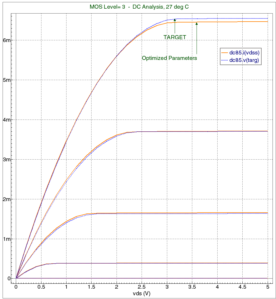
In this input deck a simple MOS level=3 device is optimized against a DATA set for a DC family of curves and the final errorlimits reported in the output log window. The optimizing parameters are: RS, RD, LD, NSUB, VTO, UO, VMAX, XJ, ETA and THETA with their defined limits set in the input deck for this simple MOS model. The final set of DC sweeps for optimized vs target are shown in plot .
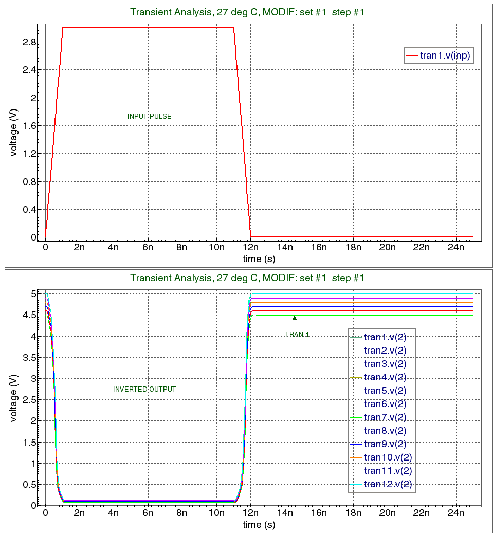
Doing an optimization of the rise and fall of a simple inverter circuit this input deck uses a basic NMOS and PMOS level 3 device to form an inverter. An optimization is done on the rise and fall times for this inverter circuit over a variation in supply voltage and the resulting plot shows the final waveforms and the data printed in the output log window of the GUI.
opMOS3.in
											** MOSFET Level 3
*  i(vds) Optimization
*****Circuit
vgs   2  0
vds   1  3
vdss  0  3   DC 0
vbs   4  0   0
m1 1 2 0 4 nm  W= 5E-05  L= 2E-06  NRD= 4E-02  NRS= 4E-02
***** MOSFET model definition
.MODEL nm NMOS ( TOX = 5E-8
+ RS = 2 RD = 2 LD = 1E-7
+ WD = 0 NSUB = 1E16 VTO = 0.8
+ UO = 626 VMAX = 2e6 XJ = 3E-7
+ ETA = 0.02 THETA = 0.03  NFS = 3E11
+ IS = 1.78E-16 CJ = 4.550487E-5 PB = 0.6172644
+ MJ = 0.4086356 FC = 0.5 CJSW = 1.876352E-10
+ MJSW = 0.4232647 CGSO = 1E-9 CGDO = 1E-9
+ CGBO = 1E-9 LEVEL = 3 )
***** Analysis and Measure statements
.DC  vds  0  5.0    0.2     vgs  1.0  5.0 1.0
.MEAS DC differr ERR2 targ i(vdss) VAL=1.e-4 NEST=-1
***** Optimization specification
.MODIF
+    OPTIMIZE
+        nm(RS) = OPT(0.01 100 2)
+        nm(RD) = OPT(0.01 100 2)
+        nm(LD) = OPT(1e-9 2e-6 1e-7)
+        nm(NSUB) = OPT(1e15 1e17 1e16)
+        nm(VTO) = OPT(0.333 2.0 0.8)
+        nm(UO) = OPT(100 800 626)
+        nm(VMAX) = OPT(1e4 1e7 2e6)
+        nm(XJ) = OPT(2e-7 3e-6 3e-7)
+        nm(ETA) = OPT(1e-4 5.0 0.02)
+        nm(THETA) = OPT(1.e-4 1 0.03)
+    TARGETS  differr=0.01
+    OPTIONS NUMITER=25 IPLOFF=1 MEASOFF=1
*
.IPLOT i(vdss) targ
.OPTIONS iplot_one nomod
***** Measured curves
.DATA  i_vds_data
+     vds           targ
+      0            1E-25
+      0.1          1.0766E-7
+      0.2          1.0797E-7
+      0.3          1.0828E-7
+      0.4          1.0859E-7
+      0.5          1.089E-7
+      0.6          1.0921E-7
+      0.7          1.0953E-7
+      0.8          1.0984E-7
+      0.9          1.1015E-7
+      1            1.1047E-7
+      1.1          1.1079E-7
+      1.2          1.1111E-7
+      1.3          1.1142E-7
+      1.4          1.1174E-7
+      1.5          1.1207E-7
+      1.6          1.1239E-7
+      1.7          1.1271E-7
+      1.8          1.1303E-7
+      1.9          1.1336E-7
+      2            1.1368E-7
+      2.1          1.1401E-7
+      2.2          1.1434E-7
+      2.3          1.1466E-7
+      2.4          1.1499E-7
+      2.5          1.1532E-7
+      2.6          1.1565E-7
+      2.7          1.1599E-7
+      2.8          1.1632E-7
+      2.9          1.1665E-7
+      3            1.1699E-7
+      3.1          1.1732E-7
+      3.2          1.1766E-7
+      3.3          1.18E-7
+      3.4          1.1834E-7
+      3.5          1.1868E-7
+      3.6          1.1902E-7
+      3.7          1.1936E-7
+      3.8          1.197E-7
+      3.9          1.2004E-7
+      4            1.2039E-7
+      4.1          1.2073E-7
+      4.2          1.2108E-7
+      4.3          1.2143E-7
+      4.4          1.2178E-7
+      4.5          1.2213E-7
+      4.6          1.2248E-7
+      4.7          1.2283E-7
+      4.8          1.2318E-7
+      4.9          1.2353E-7
+      5            1.2389E-7
+               0            1E-25
+      0.1          9.3137E-5
+      0.2          1.731E-4
+      0.3          2.3991E-4
+      0.4          2.936E-4
+      0.5          3.342E-4
+      0.6          3.6173E-4
+      0.7          3.7621E-4
+      0.8          3.787E-4
+      0.9          3.7882E-4
+      1            3.7895E-4
+      1.1          3.7908E-4
+      1.2          3.7921E-4
+      1.3          3.7934E-4
+      1.4          3.7946E-4
+      1.5          3.7959E-4
+      1.6          3.7972E-4
+      1.7          3.7985E-4
+      1.8          3.7998E-4
+      1.9          3.801E-4
+      2            3.8023E-4
+      2.1          3.8036E-4
+      2.2          3.8049E-4
+      2.3          3.8062E-4
+      2.4          3.8075E-4
+      2.5          3.8087E-4
+      2.6          3.81E-4
+      2.7          3.8113E-4
+      2.8          3.8126E-4
+      2.9          3.8139E-4
+      3            3.8151E-4
+      3.1          3.8164E-4
+      3.2          3.8177E-4
+      3.3          3.819E-4
+      3.4          3.8203E-4
+      3.5          3.8216E-4
+      3.6          3.8229E-4
+      3.7          3.8241E-4
+      3.8          3.8254E-4
+      3.9          3.8267E-4
+      4            3.828E-4
+      4.1          3.8293E-4
+      4.2          3.8306E-4
+      4.3          3.8319E-4
+      4.4          3.8331E-4
+      4.5          3.8344E-4
+      4.6          3.8357E-4
+      4.7          3.837E-4
+      4.8          3.8383E-4
+      4.9          3.8396E-4
+      5            3.8409E-4
+               0            1E-25
+      0.1          1.9906E-4
+      0.2          3.85E-4
+      0.3          5.5783E-4
+      0.4          7.176E-4
+      0.5          8.6431E-4
+      0.6          9.98E-4
+      0.7          1.1187E-3
+      0.8          1.2264E-3
+      0.9          1.3212E-3
+      1            1.403E-3
+      1.1          1.472E-3
+      1.2          1.5281E-3
+      1.3          1.5713E-3
+      1.4          1.6017E-3
+      1.5          1.6193E-3
+      1.6          1.6243E-3
+      1.7          1.6246E-3
+      1.8          1.6248E-3
+      1.9          1.6251E-3
+      2            1.6253E-3
+      2.1          1.6256E-3
+      2.2          1.6259E-3
+      2.3          1.6261E-3
+      2.4          1.6264E-3
+      2.5          1.6267E-3
+      2.6          1.6269E-3
+      2.7          1.6272E-3
+      2.8          1.6274E-3
+      2.9          1.6277E-3
+      3            1.628E-3
+      3.1          1.6282E-3
+      3.2          1.6285E-3
+      3.3          1.6288E-3
+      3.4          1.629E-3
+      3.5          1.6293E-3
+      3.6          1.6295E-3
+      3.7          1.6298E-3
+      3.8          1.6301E-3
+      3.9          1.6303E-3
+      4            1.6306E-3
+      4.1          1.6309E-3
+      4.2          1.6311E-3
+      4.3          1.6314E-3
+      4.4          1.6316E-3
+      4.5          1.6319E-3
+      4.6          1.6322E-3
+      4.7          1.6324E-3
+      4.8          1.6327E-3
+      4.9          1.633E-3
+      5            1.6332E-3
+               0            1E-25
+      0.1          3.0207E-4
+      0.2          5.9105E-4
+      0.3          8.6699E-4
+      0.4          1.1299E-3
+      0.5          1.3798E-3
+      0.6          1.6168E-3
+      0.7          1.8408E-3
+      0.8          2.0519E-3
+      0.9          2.25E-3
+      1            2.4354E-3
+      1.1          2.6078E-3
+      1.2          2.7675E-3
+      1.3          2.9143E-3
+      1.4          3.0484E-3
+      1.5          3.1697E-3
+      1.6          3.2783E-3
+      1.7          3.3742E-3
+      1.8          3.4574E-3
+      1.9          3.528E-3
+      2            3.5859E-3
+      2.1          3.6312E-3
+      2.2          3.664E-3
+      2.3          3.6842E-3
+      2.4          3.6918E-3
+      2.5          3.6922E-3
+      2.6          3.6926E-3
+      2.7          3.693E-3
+      2.8          3.6934E-3
+      2.9          3.6938E-3
+      3            3.6942E-3
+      3.1          3.6946E-3
+      3.2          3.695E-3
+      3.3          3.6954E-3
+      3.4          3.6958E-3
+      3.5          3.6962E-3
+      3.6          3.6966E-3
+      3.7          3.697E-3
+      3.8          3.6973E-3
+      3.9          3.6977E-3
+      4            3.6981E-3
+      4.1          3.6985E-3
+      4.2          3.6989E-3
+      4.3          3.6993E-3
+      4.4          3.6997E-3
+      4.5          3.7001E-3
+      4.6          3.7005E-3
+      4.7          3.7009E-3
+      4.8          3.7013E-3
+      4.9          3.7017E-3
+      5            3.7021E-3
+               0            1E-25
+      0.1          4.0226E-4
+      0.2          7.915E-4
+      0.3          1.1677E-3
+      0.4          1.531E-3
+      0.5          1.8814E-3
+      0.6          2.2188E-3
+      0.7          2.5433E-3
+      0.8          2.855E-3
+      0.9          3.1538E-3
+      1            3.4398E-3
+      1.1          3.713E-3
+      1.2          3.9734E-3
+      1.3          4.2211E-3
+      1.4          4.4561E-3
+      1.5          4.6784E-3
+      1.6          4.888E-3
+      1.7          5.0849E-3
+      1.8          5.2692E-3
+      1.9          5.441E-3
+      2            5.6001E-3
+      2.1          5.7467E-3
+      2.2          5.8808E-3
+      2.3          6.0023E-3
+      2.4          6.1114E-3
+      2.5          6.208E-3
+      2.6          6.2921E-3
+      2.7          6.3639E-3
+      2.8          6.4232E-3
+      2.9          6.4701E-3
+      3            6.5047E-3
+      3.1          6.527E-3
+      3.2          6.537E-3
+      3.3          6.5379E-3
+      3.4          6.5384E-3
+      3.5          6.539E-3
+      3.6          6.5395E-3
+      3.7          6.54E-3
+      3.8          6.5405E-3
+      3.9          6.5411E-3
+      4            6.5416E-3
+      4.1          6.5421E-3
+      4.2          6.5426E-3
+      4.3          6.5432E-3
+      4.4          6.5437E-3
+      4.5          6.5442E-3
+      4.6          6.5448E-3
+      4.7          6.5453E-3
+      4.8          6.5458E-3
+      4.9          6.5463E-3
+      5            6.5469E-3


.END
log_diff_error
											RESULTS OF OPTIMIZATION

PARAMETERS
name                    final value   init. value
--------------------   ------------  ------------
nm(rs)              =  1.81452e+000  2.00000e+000
nm(rd)              =  1.67112e+000  2.00000e+000
nm(ld)              =  9.97810e-008  1.00000e-007
nm(nsub)            =  9.07262e+015  1.00000e+016
nm(vto)             =  1.17350e+000  8.00000e-001
nm(uo)              =  6.24629e+002  6.26000e+002
nm(vmax)            =  2.18548e+006  2.00000e+006
nm(xj)              =  2.00000e-007  3.00000e-007
nm(eta)             =  1.25611e-002  2.00000e-002
nm(theta)           =  2.72178e-002  3.00000e-002
mod1.in
											Parametric analysis
***** Circuit description
vcc vss 0  DC vccDC
vin inp 0  PULSE(0 3 0 trtf trtf  10ns 40ns)
m1 2  inp  vss  vss  pm  w=wp   l=1.6u
m2 2  inp  0    0    nm  w=30u  l=2.0u
cout  2  0  50ff
.MODEL  pm  PMOS ( level=3 tox=.02e-6
+ phi=0.576 gamma=0 vto=0 alpha=0 kappa=0)
.model  nm  NMOS ( level=3 tox=.02e-6
+ phi=0.576 gamma=0 vto=0 alpha=0 kappa=0)
***** Analysis statement
.TRAN 0.1ns 25ns
***** Measure statements
.MEASURE TRAN delrise DELAY v(inp) RISE=1 VAL=1.5
+      TARG=v(2) FALL=1 VAL='0.5*vccDC'
.MEASURE TRAN maxv2 MAX  v(2)
.MEASURE TRAN delfall DELAY v(inp) FALL=1 VAL=1.5
+      TARG=v(2) RISE=1 VAL='0.5*maxv2'
***** Parameter labels
.PARAM vccDC= 5V wp=4.9u  trtf=1ns
***** Parametric analysis  specification
.MODIF proff  prtbl m2(w)=32.6u  LOOP=6 vccDC+=(4.5)0.1v
+MODIF proff  prtbl     TEMP=75  LOOP=6 vccDC+=(4.5)0.1v
.options nomod
.END
parameter_measurements
											                           TABLE OF RESULTS FOR SET #1

                           PARAMETERS and MEASUREMENTS

         m2(w)         vccdc        delrise        maxv2        delfall
     ------------  ------------  ------------  ------------  ------------

  1   3.2600e-005   4.5000e+000   2.4723e-011   4.5067e+000   1.8734e-010
  2   3.2600e-005   4.6000e+000   3.4061e-011   4.6066e+000   1.8112e-010
  3   3.2600e-005   4.7000e+000   4.3486e-011   4.7066e+000   1.7822e-010
  4   3.2600e-005   4.8000e+000   5.2992e-011   4.8065e+000   1.7475e-010
  5   3.2600e-005   4.9000e+000   6.2271e-011   4.9064e+000   1.6686e-010
  6   3.2600e-005   5.0000e+000   7.1588e-011   5.0064e+000   1.5653e-010


                           TABLE OF RESULTS FOR SET #2

                           PARAMETERS and MEASUREMENTS

         temp          vccdc        delrise        maxv2        delfall
     ------------  ------------  ------------  ------------  ------------

  1   7.5000e+001   4.5000e+000   3.1470e-011   4.5041e+000   2.0784e-010
  2   7.5000e+001   4.6000e+000   4.0800e-011   4.6040e+000   2.0012e-010
  3   7.5000e+001   4.7000e+000   5.0212e-011   4.7040e+000   1.9326e-010
  4   7.5000e+001   4.8000e+000   5.9248e-011   4.8040e+000   1.8748e-010
  5   7.5000e+001   4.9000e+000   6.7632e-011   4.9040e+000   1.8781e-010
  6   7.5000e+001   5.0000e+000   7.5901e-011   5.0040e+000   1.8382e-010
001_mos_op
[an error occurred while processing this directive]