017_jitter_noise : Noise Jitter influences
Requires: SmartSpice & Smartview
Minimum Versions: SMARTSPICE 4.6.5.R
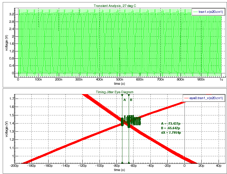
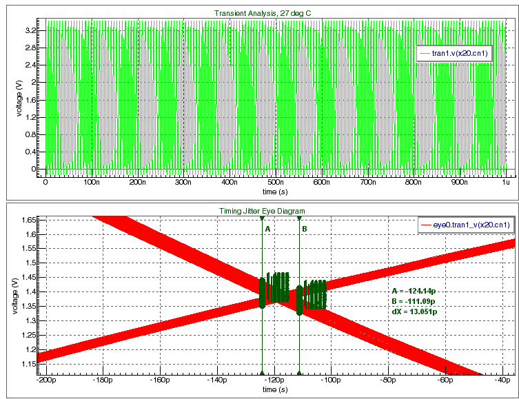
A simple 9 Stage inverting Ring Oscillator is used with an external N element noise source injected through a capacitor to show jitter sensitivity in the ring oscillator output. The input deck input deck contains .TRAN NOISE and .MEASURE analysis.
Rubberband the C2 device capacitance [cap] parameter to see the influence of injecting a different noise level on the performance and EYE diagram of the node v(x20.cn1) and you will see with no external noise source waveforms and with the injected noise waveforms visable.
Input Files
9_stage_ring_plus_noise.in
											** 9 Stage Ring Oscillator + injected N element Noise
*******************************************************cs
.ic cn23='vsupply/2'
.param vsupply=3.3
.global 0 vcc
**.include "./Pch.M"
**.include "./Nch.M"
.include "./pmos.model"
.include "./nmos.model"

** Subcircuit: Inverter
.subckt Inverter ip_inv op_inv
    C1 ip_inv 0 10f
    R1 cn19 op_inv r=10.0m
    R2 op_inv cn20 r=10.0m
    M1 cn20 ip_inv 0 0 Nch w=5u l=1.2u
    M2 vcc ip_inv cn19 vcc Pch w=10u l=1.2u
.ends Inverter

** Subcircuit: 9 Stage Ring
.subckt 9stage_inverter_block in out
    R3  in   cn1 r=2
    R4  cn2  cn3 r=2
    R5  cn4  cn5 r=2
    R6  cn6  cn7 r=2
    R7  cn8  cn9 r=2
    R8  cn10 cn11 r=2
    R9  cn12 cn13 r=2
    R10 cn14 cn15 r=2
    R11 cn16 cn17 r=2
    R12 cn18  out r=2
    X1 cn1  cn2  Inverter
    X2 cn3  cn4  Inverter
    X3 cn5  cn6  Inverter
    X4 cn7  cn8  Inverter
    X5 cn9  cn10 Inverter
    X6 cn11 cn12 Inverter
    X7 cn13 cn14 Inverter
    X8 cn15 cn16 Inverter
    X9 cn17 cn18 Inverter
.ends 9stage_inverter_block

** Buffer output from ring
.subckt buffer_stage in_buf out_buf
    M1 cn30 in_buf 0 0 Nch w=5u l=1.2u
    M2 vcc in_buf cn30 vcc Pch w=10u l=1.2u
    M3 out_buf cn30 0 0 Nch w=10u l=1.2u
    M4 vcc cn30 out_buf vcc Pch w=20u l=1.2u
.ends buffer_stage

** Main Circuit

X20  cn27   cn23 9stage_inverter_block
X21  cn23   cn24 buffer_stage
**V0   cn27     0  pulse( 0.0 vsupply 0.0 1.5e-9 1.5e-9 8e-9 20e-9)
R1   cn27  cn23  1
C0   cn49     0  c=2p
R2   cn24  cn49  r=100
V1   vcc      0  dc=vsupply

** Noise element
N   cn28    0  SW=1.6632e-21
C2  cn28 cn27  0.2pF

.save  V(cn27) V(cn27)

.TRAN 10p 1u  Jitter NOISE   noiseseed=1 noisefmax=5e9 noisescale=1.0

.measure PPvoltage  PP v(SM)   FROM=0n TO=1u
.measure RMSvoltage RMS v(SM)  FROM=0n TO=1u


*.tran 0.1n 300n

.save v(x20.cn1)  v(x20.cn3)  v(x20.cn5)  v(x20.cn7)  v(x20.cn9)
.save v(x20.cn11) v(x20.cn13) v(x20.cn15) v(x20.cn17) v(x20.cn18)
.save v(x21.cn23) v(x21.cn24)

.save all(v)

.end
Graphics