13 : Faster Extraction of Designs with Large Amounts of Filling Metals
Minimum Required Versions: Expert 5.2204.3.R, Hipex 3.8.7.R
In the normal operation, Hipex-RC treats all dummy metal patterns as the normal conductor (the same way as interconnect wires). It causes a lot of nodes and parasitic devices, which increases the processing time not only for the parasitic extraction but also for the post-layout simulation.
To optimize the performance, those dummy metal patterns can be treated as a special shield layer. The dummy metal between two interconnect wires or between a interconnect wire and the substrate layer increases the total permittivity and causes higher parasitic capacitances.
So, different coefficient values may be applied for a couple of interconnect layers where dummy metal patterns are overlapping, such as the followings:
cpx Area metal2 substrate
1.04324e-005 * 1.59654
/outside_layers=metal1_dummy
;
cpx Fringe metal2 substrate
(3.25999e-005 * 1.59654),0.182479,1.11013
/outside_layers=metal1_dummy
/max_distance = 3
/max_width = 0
;
cpx Area metal2 substrate
1.04324e-005
;
cpx Fringe metal2 substrate
3.25999e-005,0.182479,1.11013
/max_distance = 3
/max_width = 0
;
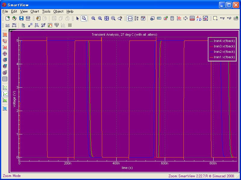
Reduction of the number of nodes to be treated in the parasitic extraction makes the processing faster with fewer parasitic devices. It also reduces the processing time for the post-layout simulation effectively. The figure0 shows the results of the post-layout simulation with the following netlists:
tran1 : without parasitic RCs
tran2 : with parasitic RCs excluding dummy metals
tran3 : with parasitic RCs including dummy metals treated as normal interconnects
tran4 : with parasitic RCs including dummy metals treated as "outside_layers"
The results are almost same between the case where the dummy metals are treated as normal interconnects (tran3) and the case where they are treated as the "outside_layers" to increase the permittivity (tran4).
The actual operation steps are as follows:
1) Start Expert.
2) Go to File->Open , and load the project file h_13_1.eld.
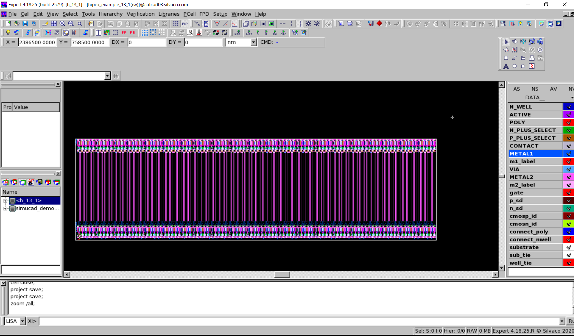
3) Open the top cell hipex_example_13_1 in Open Cell(s) dialog. It includes a layout design of ring oscillator without dummy metal pattern ( figure1 ).
4) Select Verification->Extraction->Setup to open the "Layout Parameter Extraction Setup" dialog. Press Load button, and choose hipex_example_13_1.lpe file to load required extraction settings.
Open "Technology" page, and make sure that a parasitic capacitance technology file without_dummy.cmd is specified.
5) Select Verification->Extraction->Hipex-net->Run to obtain a SPICE netlist not including parasitic devices.
6) Select Verification->Extraction->Hipex-RC->Run to obtain a SPICE netlist containing parasitic RC devices.
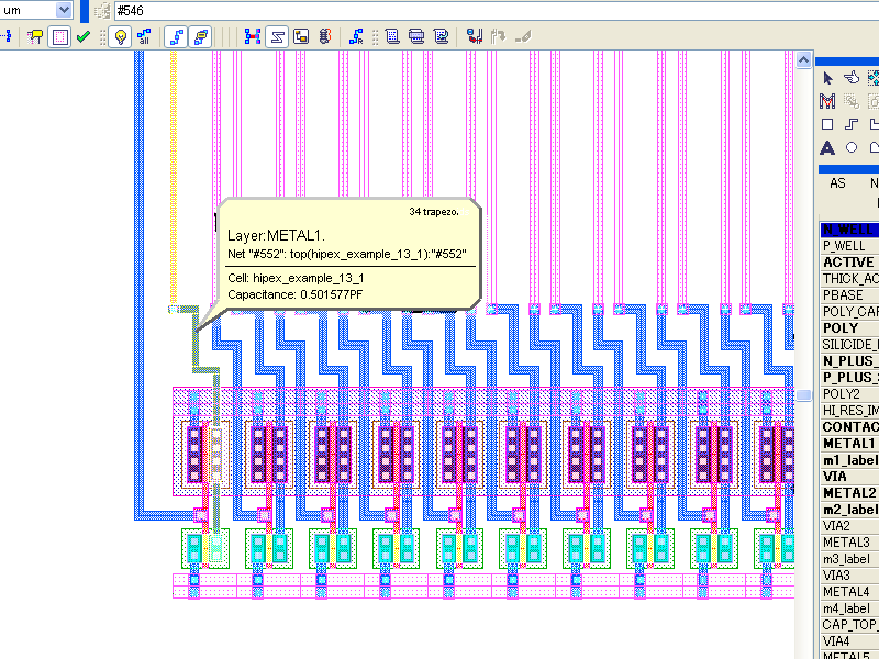
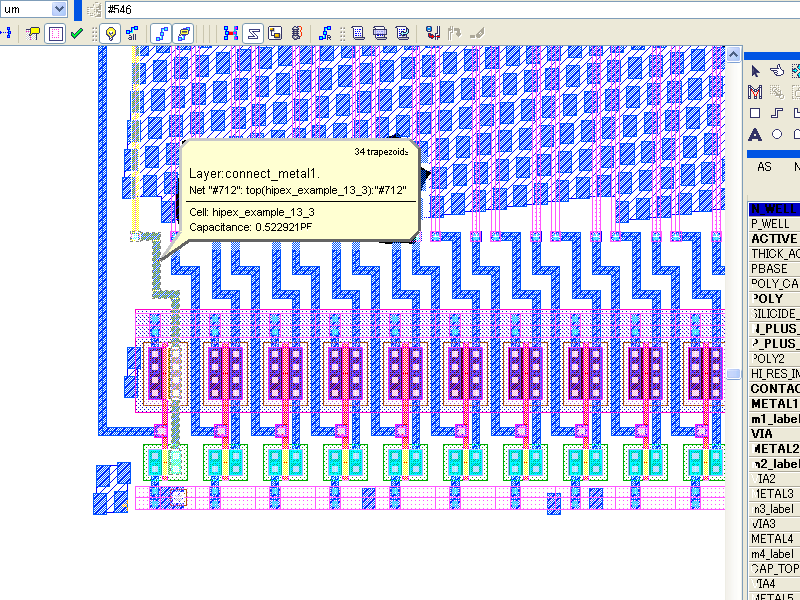
7) Select Verification->Node-Probing->Pick Node , and click the interconnect wire at the left bottom. The value of the extracted parasitic capacitance will be indicated ( figure2 ).
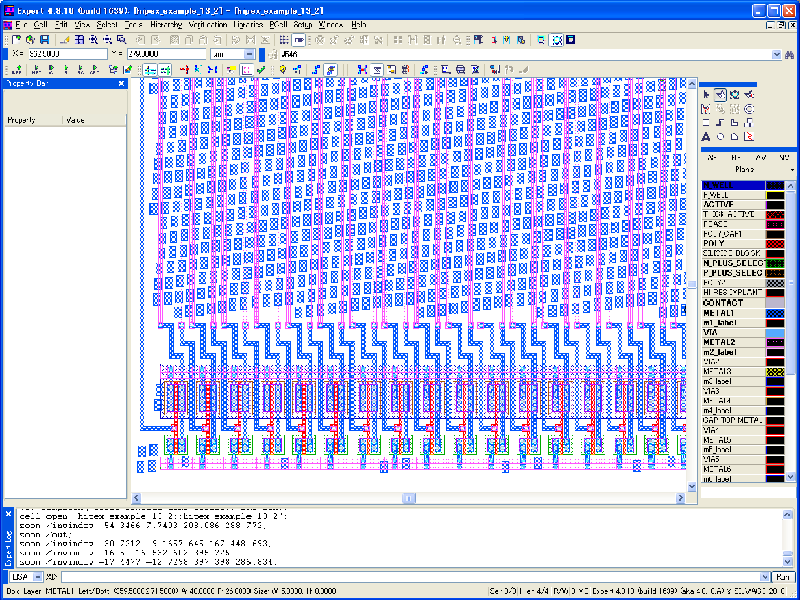
8) Go to File->Open , load another project file h_13_2.eld, and open the top cell hipex_example_13_2, which includes dummy metal patterns ( figure3 ). Select Verification->Extraction->Setup to open the "Layout Parameter Extraction Setup" dialog. Press Load button, and choose hipex_example_13_2.lpe file to load required extraction settings.
9) Select Verification->Extraction->Hipex-net->Run , and Verification->Extraction->Hipex-RC->Run in the same way as 5) and 6). The processing time will be almost doubled than that of the previous processing, because of much more nodes and parasitic devices generated.
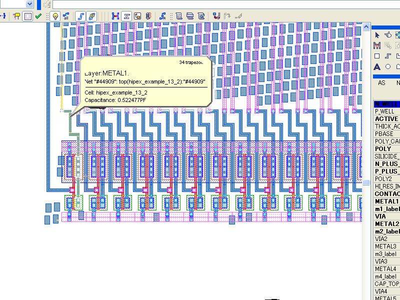
10) Select Verification->Node-Probing->Pick Node, and click the interconnect wire at the left bottom again. The value of the extracted parasitic capacitance will be greater than the previous one ( figure4 ).
11) Go to File->Open , load another project file h_13_3.eld , and open the top cell "hipex_example_13_3". The layout design is completely same as the previous one, but has some different settings for processing of dummy metal patterns.
12) Select Verification->Extraction->Setup to open the "Layout Parameter Extraction Setup" dialog. Press Load button, and choose hipex_example_13_3.lpe file to load required extraction settings. Then open "Technology" page, and make sure that a parasitic capacitance technology file with_dummy.cmd is specified.
13) Select Verification->Extraction->Hipex-net->Run , and Verification->Extraction->Hipex-RC->Run in the same way as 5) and 6). The processing time will be recovered to the same time as the first processing, because the number of parasitic RC devices are reduced by the setting of dummy metal patterns.
14) Select Verification->Node-Probing->Pick Node , and click the interconnect wire at the left bottom again. The value of the extracted parasitic capacitance will be almost same as the previous one ( figure5 ).
h_13_1.dsf
											//  Layer generation for 'h_13_1' project
//  Number of derived layers: 39

Select: Layer1=PBASE, Layer2=N_PLUS_SELECT, LayerR=&PNP_PBASE, Relation=overlap, options=(not);
UnderSize: Value=1um, Layer=&PNP_PBASE, LayerR=&A;
Logicform: pnp_id=&A.dif.(ACTIVE);

Contours: Layer=pnp_id, LayerR=pnp_e, options=(holes);
Logicform: pnp_c=PBASE.and.ACTIVE.dif.(pnp_e.or.P_PLUS_SELECT.or.N_PLUS_SELECT);

Logicform: npn_e=PBASE.and.N_PLUS_SELECT.AND.ACTIVE;
LogicForm: npn_b=PBASE.and.ACTIVE.and.P_PLUS_SELECT;
Logicform: gate=POLY.and.ACTIVE;
Logicform: p_sd=(P_PLUS_SELECT.and.ACTIVE.AND.N_WELL).dif.(POLY.or.DEEP_N_WELL.or.RES_ID);
Logicform: n_sd=(N_PLUS_SELECT.and.ACTIVE).dif.(POLY.or.THICK_ACTIVE.or.N_WELL);
Logicform: cmosp_id=gate.and.P_PLUS_SELECT.and.N_WELL;
Logicform: cmosn_id=gate.and.N_PLUS_SELECT.dif.THICK_ACTIVE;
Logicform: hvcmosp_id=gate.and.P_PLUS_SELECT.and.THICK_ACTIVE.dif.P_WELL;
Select: Layer1=ACTIVE, Layer2=hvcmosp_id, Relation=overlap, LayerR=&A;
Logicform: hvpmos_d=&A.dif.(POLY.or.P_WELL.or.N_WELL);
Select: Layer1=ACTIVE, Layer2=hvcmosp_id, Relation=overlap, LayerR=&A;
Logicform: hvpmos_s=&A.dif.(hvcmosp_id.or.N_WELL.or.hvpmos_d);
Logicform: hvcmosn_id=gate.and.N_PLUS_SELECT.and.THICK_ACTIVE;
Select: Layer1=ACTIVE, Layer2=hvcmosn_id, Relation=overlap, LayerR=&A;
Logicform: hvnmos_d=&A.dif.(POLY.or.P_PLUS_SELECT.or.N_WELL);
Select: Layer1=ACTIVE, Layer2=hvcmosn_id, Relation=overlap, LayerR=&A;
Logicform: hvnmos_s=&A.dif.(hvcmosn_id.or.hvnmos_d.or.P_PLUS_SELECT);
Logicform: rpplus_id=N_WELL.and.P_PLUS_SELECT.and.ACTIVE.and.RES_ID;
Logicform: rnpoly_id=N_PLUS_SELECT.and.POLY.and.RES_ID;
Logicform: rpoly_id=(POLY.and.RES_ID).dif.N_PLUS_SELECT;
Logicform: rnwell_id=(N_WELL.and.RES_ID).dif.P_PLUS_SELECT;
LogicForm: &rpplus_pin1=(ACTIVE.and.P_PLUS_SELECT).dif.RES_ID;
Select: Relation=touch, Layer1=&rpplus_pin1, Layer2=rpplus_id, LayerR=rpplus_pin;
Logicform: connect_poly=POLY.dif.RES_ID;
Logicform: connect_nwell=N_WELL.dif.(RES_ID);
Substrate: LayerR=substrate;
Logicform: sub_tie=(ACTIVE.AND.P_PLUS_SELECT).dif.(DEEP_N_WELL.or.N_WELL);
Logicform: well_tie=(ACTIVE.AND.N_PLUS_SELECT.AND.N_WELL).dif.npn_e;
Logicform: &deepnwell_tie1=ACTIVE.AND.N_PLUS_SELECT.AND.DEEP_N_WELL;
Select: Relation=touch, Layer1=&deepnwell_tie1, Layer2=hvpmos_s, LayerR=&temp;
LogicForm: deepnwell_tie=&deepnwell_tie1.dif.&temp;
Logicform: p1p2_id=(POLY2.and.POLY).dif.ACTIVE;
Logicform: poly_con=(POLY.dif.POLY2).and.CONTACT;
Logicform: poly2cap_con=POLY.AND.POLY2.and.CONTACT;
LogicForm: &ind_id1=METAL1.and.INDDMY_ID;
PERIMETER: Layer=&ind_id1, Value=75, Type=GT, LayerR=ind_id;
Corner: Layer=ind_id, Value=0.2, Options=(inside,A90), LayerR=&temp1;
Select: Relation=flush, Layer1=&temp1, Layer2=INDDMY_ID, LayerR=&temp2;
Size: Layer=&temp2, within=ind_id, Options=(cut), step=0.5, Value=10, LayerR=ind_plus;
Select: Relation=cut, Layer1=METAL2, Layer2=ind_id, LayerR=ind_minus;
Corner: Layer=ind_id, Value=0.1, Options=(inside,any), LayerR=NR_counter;
LogicForm: width=METAL1.and.METAL2.and.INDDMY_ID;
LogicForm: &space1=(METAL2.and.INDDMY_ID).dif.METAL1;
PERIMETER: Layer=&space1, LayerR=&space2, Value=79, Type=LT;
SELECT: Relation=touch, layer1=&space2, Layer2=ind_id, LayerR=&space3;
SELECT_edges: Relation=coincide, layer1=&space3, Layer2=ind_id, LayerR=&space4;
SELECT: Relation=touch, layer1=&space3, Layer2=&space4, LayerR=space, options=(2:2);
LogicForm: &space1=(METAL2.and.INDDMY_ID).dif.METAL1;
PERIMETER: Layer=&space1, LayerR=radius, Value=80, Type=GE;
And: layer1=METAL1, layer2=newcell7_boundary, layerR=&tmp1;
Select: Relation=LABEL, Layer1=&tmp1, Layer2=m1_label, LIST=(C),
         LayerR=pinC;

And: layer1=METAL1, layer2=newcell7_boundary, layerR=&tmp1;
Select: Relation=LABEL, Layer1=&tmp1, Layer2=m1_label, LIST=(B),
         LayerR=pinB;
h_13_1_net_cmd.lisa
											!--------------------------------------------------------------------
!Net command file
!DESIGN    : design
!TECHNO    : techno
!USER      :
!TIME      : Wed May 20 22:19:11 2020

!--------------------------------------------------------------------

! HIPEX to CUP map table

cup layer "poly1" /hipex_layer="connect_poly";
cup layer "metal4" /hipex_layer="METAL4";
cup layer "metal5" /hipex_layer="METAL5";
cup layer "metal6" /hipex_layer="METAL6";
cup layer "metal1" /hipex_layer="METAL1";
cup layer "metal2" /hipex_layer="METAL2";
cup layer "metal3" /hipex_layer="METAL3";
cup layer "substrate" /hipex_layer="substrate";

! GDS LAYER MAP

hipex layer /gds_layer=   0 /gds_type= 0 /geom_layer="connect_nwell";
hipex layer /gds_layer=   1 /gds_type= 0 /geom_layer="connect_poly";
hipex layer /gds_layer=   2 /gds_type= 0 /geom_layer="rpplus_pin";
hipex layer /gds_layer=   3 /gds_type= 0 /geom_layer="rnwell_id";
hipex layer /gds_layer=   4 /gds_type= 0 /geom_layer="rpoly_id";
hipex layer /gds_layer=   5 /gds_type= 0 /geom_layer="rnpoly_id";
hipex layer /gds_layer=   6 /gds_type= 0 /geom_layer="rpplus_id";
hipex layer /gds_layer=   7 /gds_type= 0 /geom_layer="hvnmos_s";
hipex layer /gds_layer=   8 /gds_type= 0 /geom_layer="hvnmos_d";
hipex layer /gds_layer=   9 /gds_type= 0 /geom_layer="hvcmosn_id";
hipex layer /gds_layer=  10 /gds_type= 0 /geom_layer="hvpmos_s";
hipex layer /gds_layer=  11 /gds_type= 0 /geom_layer="hvpmos_d";
hipex layer /gds_layer=  12 /gds_type= 0 /geom_layer="hvcmosp_id";
hipex layer /gds_layer=  13 /gds_type= 0 /geom_layer="cmosn_id";
hipex layer /gds_layer=  14 /gds_type= 0 /geom_layer="cmosp_id";
hipex layer /gds_layer=  15 /gds_type= 0 /geom_layer="n_sd";
hipex layer /gds_layer=  16 /gds_type= 0 /geom_layer="p_sd";
hipex layer /gds_layer=  17 /gds_type= 0 /geom_layer="npn_b";
hipex layer /gds_layer=  18 /gds_type= 0 /geom_layer="npn_e";
hipex layer /gds_layer=  19 /gds_type= 0 /geom_layer="pnp_c";
hipex layer /gds_layer=  20 /gds_type= 0 /geom_layer="pnp_e";
hipex layer /gds_layer=  21 /gds_type= 0 /geom_layer="pnp_id";
hipex layer /gds_layer=  22 /gds_type= 0 /geom_layer="m3_label";
hipex layer /gds_layer=  23 /gds_type= 0 /text_layer="m2_label";
hipex layer /gds_layer=  24 /gds_type= 0 /text_layer="m1_label";
hipex layer /gds_layer=  25 /gds_type= 0 /geom_layer="CONTACT";
hipex layer /gds_layer=  30 /gds_type= 0 /geom_layer="VIA3";
hipex layer /gds_layer=  31 /gds_type= 0 /geom_layer="METAL4";
hipex layer /gds_layer=  32 /gds_type= 0 /geom_layer="VIA4";
hipex layer /gds_layer=  33 /gds_type= 0 /geom_layer="METAL5";
hipex layer /gds_layer=  36 /gds_type= 0 /geom_layer="VIA5";
hipex layer /gds_layer=  37 /gds_type= 0 /geom_layer="METAL6";
hipex layer /gds_layer=  38 /gds_type= 0 /geom_layer="DEEP_N_WELL";
hipex layer /gds_layer=  46 /gds_type= 0 /geom_layer="POLY";
hipex layer /gds_layer=  49 /gds_type= 0 /geom_layer="METAL1";
hipex layer /gds_layer=  50 /gds_type= 0 /geom_layer="VIA";
hipex layer /gds_layer=  51 /gds_type= 0 /geom_layer="METAL2";
hipex layer /gds_layer=  56 /gds_type= 0 /geom_layer="POLY2";
hipex layer /gds_layer=  58 /gds_type= 0 /geom_layer="PBASE";
hipex layer /gds_layer=  61 /gds_type= 0 /geom_layer="VIA2";
hipex layer /gds_layer=  62 /gds_type= 0 /geom_layer="METAL3";
hipex layer /gds_layer=  63 /gds_type= 0 /geom_layer="substrate";
hipex layer /gds_layer=  64 /gds_type= 0 /geom_layer="sub_tie";
hipex layer /gds_layer=  65 /gds_type= 0 /geom_layer="well_tie";
hipex layer /gds_layer=  66 /gds_type= 0 /geom_layer="deepnwell_tie";
hipex layer /gds_layer=  67 /gds_type= 0 /geom_layer="p1p2_id";
hipex layer /gds_layer=  68 /gds_type= 0 /geom_layer="poly_con";
hipex layer /gds_layer=  69 /gds_type= 0 /geom_layer="poly2cap_con";
hipex layer /gds_layer=  70 /gds_type= 0 /geom_layer="ind_plus";
hipex layer /gds_layer=  71 /gds_type= 0 /geom_layer="ind_minus";
hipex layer /gds_layer=  72 /gds_type= 0 /geom_layer="HPX$npn_e";

! TEXT TYPES


! PORT LAYERS

hipex port_layer "m1_label";
hipex port_layer "m2_label";

! SOFT LAYERS


! MISC (optional) statementsS


! CONNECTIVITY

hipex connect "DEEP_N_WELL" "deepnwell_tie";
hipex connect "METAL1" "POLY2" /contact="poly2cap_con";
hipex connect "METAL1" "METAL2" /contact="VIA";
hipex connect "METAL1" "pnp_e" /contact="CONTACT";
hipex connect "METAL1" "pnp_c" /contact="CONTACT";
hipex connect "METAL1" "npn_e" /contact="CONTACT";
hipex connect "METAL1" "npn_b" /contact="CONTACT";
hipex connect "METAL1" "p_sd" /contact="CONTACT";
hipex connect "METAL1" "n_sd" /contact="CONTACT";
hipex connect "METAL1" "hvpmos_d" /contact="CONTACT";
hipex connect "METAL1" "hvpmos_s" /contact="CONTACT";
hipex connect "METAL1" "hvnmos_d" /contact="CONTACT";
hipex connect "METAL1" "hvnmos_s" /contact="CONTACT";
hipex connect "METAL1" "rpplus_pin" /contact="CONTACT";
hipex connect "METAL1" "connect_poly" /contact="poly_con";
hipex connect "METAL1" "sub_tie" /contact="CONTACT";
hipex connect "METAL1" "well_tie" /contact="CONTACT";
hipex connect "METAL1" "ind_plus";
hipex attach "m1_label" "METAL1";
hipex connect "METAL2" "METAL3" /contact="VIA2";
hipex attach "m2_label" "METAL2";
hipex connect "METAL3" "METAL4" /contact="VIA3";
hipex connect "METAL4" "METAL5" /contact="VIA4";
hipex connect "METAL5" "METAL6" /contact="VIA5";
hipex connect "PBASE" "npn_b";
hipex connect "connect_nwell" "well_tie";
hipex connect "connect_poly" "POLY";
hipex connect "deepnwell_tie" "METAL1" /contact="CONTACT";
hipex connect "substrate" "sub_tie";

! DEVICES TEXTS


! DEVICE DEFINITIONS

hipex define_device PMOS "cmosp_id" /drain="p_sd" /gate="connect_poly" /source="p_sd" /subs="connect_nwell" /model_name="CMOSP";
hipex define_device NMOS "cmosn_id" /drain="n_sd" /gate="connect_poly" /source="n_sd" /subs="substrate" /model_name="CMOSN";
hipex define_device C "p1p2_id" /pin1="POLY2" /pin2="connect_poly" /area_cap=0.0075 /perim_cap=0.00625 /model_name="P1P2";
hipex define_device PMOS "hvcmosp_id" /drain="hvpmos_d" /gate="connect_poly" /source="hvpmos_s" /subs="DEEP_N_WELL" /model_name="HVCMOSP";
hipex define_device NMOS "hvcmosn_id" /drain="hvnmos_d" /gate="connect_poly" /source="hvnmos_s" /subs="substrate" /model_name="HVCMOSN";
hipex define_device NPN "HPX$npn_e" /collector="connect_nwell" /base="PBASE" /emitter="npn_e" /subs="substrate" /area_unit=36 /model_name="NPN";
hipex define_device PNP "pnp_id" /collector="pnp_c" /base="connect_nwell" /emitter="pnp_e" /model_name="PNP";
hipex define_device R "rnwell_id" /pin1="well_tie" /pin2="well_tie" /subs="substrate" /cont_res=0 /delta_l=0.4 /delta_w=-0.02 /head_res=0 /sheet_res=10000 /model_name="RNWELL";
hipex define_device R "rpplus_id" /pin1="rpplus_pin" /pin2="rpplus_pin" /subs="connect_nwell" /cont_res=0 /delta_l=0.5 /delta_w=-0.05 /head_res=0 /sheet_res=200 /model_name="RPPLUS";
hipex define_device R "rnpoly_id" /pin1="connect_poly" /pin2="connect_poly" /cont_res=0 /delta_l=0.4 /delta_w=0.02 /head_res=0 /sheet_res=50 /model_name="RNPOLY";
hipex define_device R "rpoly_id" /pin1="connect_poly" /pin2="connect_poly" /cont_res=0 /delta_l=0.4 /delta_w=0.02 /head_res=0 /sheet_res=50 /model_name="RPOLY";

! GEOMETRICAL OPERATIONS

    hipex copy "npn_e" "HPX$npn_e";


! SOFT/WELL CHECKS
h_13_1_opt.lisa
											!--------------------------------------------------------------------
!Run file
!DESIGN    : design
!TECHNO    : techno
!USER      :
!TIME      : Wed May 20 22:19:41 2020

!--------------------------------------------------------------------
TOP_CELL                                = "hipex_example_13_1";

HIPEX_DB_DIRECTORY                      = "database";
!--------------------------------------------------------------------
!Extraction: LISA template command file
!--------------------------------------------------------------------

!--------------------------------------------------------------------
!Layout parameters
!--------------------------------------------------------------------
HIPEX_LAYOUT_FORMAT                     = "GDS";
HIPEX_LAYOUT_FILE                       = "hipex_example_13_1$HPX.gds";
HIPEX_OVERLAP_INSTANCE_CHECK            = "NO";
HIPEX_SUPPRESS_NOTEMPTY                 = "YES";
HIPEX_NON45_FLAG                        = "NO";

!--------------------------------------------------------------------
!Connectivity parameters
!--------------------------------------------------------------------
HIPEX_TERNARY_CONNECT_THROUGH_TOUCH     = "NO";

!--------------------------------------------------------------------
!Output parameters
!--------------------------------------------------------------------
HIPEX_COMMENT_MODEL                     = "NO";
HIPEX_COMMENT_TOP_SUBCKT                = "NO";
HIPEX_HIER_SPICE_WL_NAME                = "/home/alexa/2020_06/13/./hipex_example_13_1_hier.spice";
HIPEX_MOSFET_LW_ONLY                    = "NO";
HIPEX_MOSFET_EXCLUDE_W_SD               = "NO";
HIPEX_OUTPUT_SPICE_ATTRIBUTES           = "YES";
HIPEX_CAP_OUTPUT_LW                     = "NO";
HIPEX_RES_OUTPUT_LW                     = "YES";
HIPEX_CAP_OUTPUT_AREA_PERIMETER         = "YES";
HIPEX_OUTPUT_SPICE_FORMAT               = "HSPICE";
HIPEX_PININFO                           = "NO";
HIPEX_PRINT_MESSAGES                    = "NO";
NETLIST_OUTPUT_PM                       = "NO";
NETLIST_DISTRIBUTION_MODE               = "ACCURATE";
NETLIST_LINE_LENGTH                     = 80;
NETLIST_EXCLUDE_LIBRARY_PREFIX          = "NO";
NETLIST_GLOBALS_IN_SUBCKT_PINS          = "YES";
NETLIST_TEXTED_PINS                     = "YES";
NETLIST_LIBRARIES                       = {"simucad_demo_pcells"};

!--------------------------------------------------------------------
!ERC parameters
!--------------------------------------------------------------------
HIPEX_DANGLE_FLAG                       = "YES";
HIPEX_CAP_MESSAGE                       = "YES";
HIPEX_DIODE_MESSAGE                     = "NO";
HIPEX_RENAME_OPENS                      = "YES";
HIPEX_MULTILABEL_NAME                   = "";
HIPEX_SOFTCHECK_WARNINGS_AS_ERRORS      = "NO";

!--------------------------------------------------------------------
!Node Name parameters
!--------------------------------------------------------------------
HIPEX_HIERARCHY_SEPARATOR               = "/";
HIPEX_NODE_NAME_SEPARATOR               = "_";
HIPEX_DEFAULT_INSTANCE_PREFIX           = "I";
HIPEX_DEFAULT_NODE_PREFIX               = "#";
HIPEX_DELETE_BAD_CHAR                   = "NO";
HIPEX_XY_LOCATION                       = "NO";
HIPEX_CASE_SENSITIVE_NET_NAMES          = "YES";
HIPEX_AUTOGENERATE_LOCAL                = "YES";
POWER_NODE                              = {"VDD"};
GROUND_NODE                             = {"GND"};
GLOBAL_TEXT_LIST                        = {"GND", "VDD"};
HIPEX_PIN_DELIMITER                     = ":";

!--------------------------------------------------------------------
!Explosion parameters
!--------------------------------------------------------------------
HIPEX_WIRING_EXPLODE                    = "NO";
HIPEX_KEEP_FLATTEN_CELLS                = "YES";
HIPEX_TEXT_TOP                          = "NO";
HIPEX_AUTO_EXPLODE                      = "NO";
HIPEX SET_CELL_OPTIONS {"hipex_example_13_1"} /EXPLODE;

!--------------------------------------------------------------------
!Pins parameters
!--------------------------------------------------------------------
HIPEX_IGNORE_DANGLE_PINS                = "YES";

!--------------------------------------------------------------------
!Virtual Nets parameters
!--------------------------------------------------------------------
HIPEX_CHANGE_VIRTUAL_NETS               = "SUFFIX";
HIPEX_VIRTUAL_NET_SYMBOLS               = ":";
HIPEX_TOP_VIRTUAL_CONNECT_ONLY          = "YES";

!--------------------------------------------------------------------
!BackAnnotate parameters
!--------------------------------------------------------------------
HIPEX_BACKANNOTATE                      = "NO";

!--------------------------------------------------------------------
!Capacitance Extraction parameters
!--------------------------------------------------------------------
CPX_COUPLED_THRESHOLD                   = 0.0;
CPX_EXTRACT_DANGLES                     = "NO";
CPX_OUTPUT_DUMMY_CAPA                   = "NO";
CPX_FIELD_SOLVER                        = "NO";

!--------------------------------------------------------------------
!Field Solver C-extraction (Stellar) parameters
!--------------------------------------------------------------------
CPX_STEP_X                              = 0.5;
CPX_STEP_Y                              = 0.5;
CPX_STEP_Z                              = 0.5;
CPX_PRECISION                           = 0.01;
CPX_MAX_ITER                            = 100;
CPX_DECOMPOSITION                       = "YES";
CPX_DEC_STEP                            = "NO";
CPX_DEC_VALUE                           = -1.0;
CPX_BOX                                 = "NO";
CPX_BOX_VALUES_XMIN                     = 0.0;
CPX_BOX_VALUES_XMAX                     = 0.0;
CPX_BOX_VALUES_YMIN                     = 0.0;
CPX_BOX_VALUES_YMAX                     = 0.0;
CPX_FILTER                              = "NO";
CPX_CAPA_MIN                            = 1e-20;
CPX_RENEW                               = "NO";
CPX_SAVE_FILE                           = "/home/alexa/2020_06/13/./RenewSavedFile.sav";
CPX_THREED_GENERATION                   = "NO";
CPX_THREED_FILENAME                     = "/home/alexa/2020_06/13/./3DStructureFile.str";

!--------------------------------------------------------------------
!Field Solver C-extraction (Clever) parameters
!--------------------------------------------------------------------

!--------------------------------------------------------------------
!Resistance Extraction parameters
!--------------------------------------------------------------------
RPX_SERIAL_MERGE_THRESHOLD              = 0.0;
RPX_OUTPUT_XY                           = "NO";
RPX_OUTPUT_LAYER_NAMES                  = "NO";
RPX_SKIP_POWER                          = "YES";
RPX_USE_TEXTS_AS_SUBNODES               = "NO";
RPX_USE_FIELD_SOLVER                    = "NO";

!--------------------------------------------------------------------
!Netlist RC Reduction parameters
!--------------------------------------------------------------------
NETLIST_CRC                             = "NO";

!--------------------------------------------------------------------
!Coefficient Units parameters
!--------------------------------------------------------------------
HIPEX SET_UNIT /CAPACITANCE "pF";
HIPEX SET_UNIT /RESISTANCE "Ohm";
HIPEX SET_UNIT /LENGTH "um";
h_13_1_r_cmd.lisa
											! ========================================================== !
!   Hipex-R parasitic resistance extraction rules            !
! ========================================================== !

hipex set_unit /resistance "Ohm" ;
hipex set_unit /length "um" ;

rpx define_parasitic Contact
     /layer = CONTACT
     /top = METAL1
     /bottom = hvnmos_s
     /pres_area_resistivity_value = 1.0
;

rpx define_parasitic Contact
     /layer = CONTACT
     /top = rpplus_pin
     /bottom = METAL1
     /pres_area_resistivity_value = 1.0
;

rpx define_parasitic Contact
     /layer = CONTACT
     /top = npn_e
     /bottom = METAL1
     /pres_area_resistivity_value = 1.0
;

rpx define_parasitic Contact
     /layer = CONTACT
     /top = n_sd
     /bottom = METAL1
     /pres_area_resistivity_value = 1.0
;

rpx define_parasitic Contact
     /layer = CONTACT
     /top = pnp_c
     /bottom = METAL1
     /pres_area_resistivity_value = 1.0
;

rpx define_parasitic Contact
     /layer = CONTACT
     /top = npn_b
     /bottom = METAL1
     /pres_area_resistivity_value = 1.0
;

rpx define_parasitic Contact
     /layer = CONTACT
     /top = p_sd
     /bottom = METAL1
     /pres_area_resistivity_value = 1.0
;

rpx define_parasitic Contact
     /layer = CONTACT
     /top = sub_tie
     /bottom = METAL1
     /pres_area_resistivity_value = 1.0
;

rpx define_parasitic Contact
     /layer = CONTACT
     /top = hvpmos_s
     /bottom = METAL1
     /pres_area_resistivity_value = 1.0
;

rpx define_parasitic Contact
     /layer = CONTACT
     /top = hvpmos_d
     /bottom = METAL1
     /pres_area_resistivity_value = 1.0
;

rpx define_parasitic Contact
     /layer = CONTACT
     /top = hvnmos_d
     /bottom = METAL1
     /pres_area_resistivity_value = 1.0
;

rpx define_parasitic Contact
     /layer = CONTACT
     /top = pnp_e
     /bottom = METAL1
     /pres_area_resistivity_value = 1.0
;

rpx define_parasitic Wire
     /layer = METAL1
     /max_length = 20.0
     /contact_cluster = 2.0
     /pres_sheet_resistivity_value = 0.05
;

rpx define_parasitic Wire
     /layer = METAL2
     /max_length = 20.0
     /contact_cluster = 2.0
     /pres_sheet_resistivity_value = 0.05
;

rpx define_parasitic Contact
     /layer = VIA
     /top = METAL2
     /bottom = METAL1
     /pres_area_resistivity_value = 1.0
;

rpx define_parasitic Contact
     /layer = VIA2
     /top = METAL3
     /bottom = METAL2
     /pres_area_resistivity_value = 1.0
;

rpx define_parasitic Contact
     /layer = VIA3
     /top = METAL4
     /bottom = METAL3
     /pres_area_resistivity_value = 1.0
;

rpx define_parasitic Contact
     /layer = VIA4
     /top = METAL5
     /bottom = METAL4
     /pres_area_resistivity_value = 1.0
;

rpx define_parasitic Contact
     /layer = VIA5
     /top = METAL6
     /bottom = METAL5
     /pres_area_resistivity_value = 1.0
;

rpx define_parasitic Wire
     /layer = connect_poly
     /max_length = 20.0
     /contact_cluster = 2.0
     /pres_sheet_resistivity_value = 40.0
;

rpx define_parasitic Contact
     /layer = poly2cap_con
     /top = POLY2
     /bottom = METAL1
     /pres_area_resistivity_value = 1.0
;

rpx define_parasitic Contact
     /layer = poly_con
     /top = connect_poly
     /bottom = METAL1
     /pres_area_resistivity_value = 1.0
;
run_net.lisa
											INCLUDE ("h_13_3_opt.lisa");
INCLUDE ("h_13_3_net_cmd.lisa");

HIPEX_SUMMARY_PATH                      = "/home/alexa/2020_06/13";
HIPEX_NET_MAIN();
run_rc.lisa
											INCLUDE ("h_13_3_opt.lisa");
INCLUDE ("h_13_3_net_cmd.lisa");
INCLUDE ("h_13_3_r_cmd.lisa");
INCLUDE ("../with_dummy.cmd");

HDB READ;
print("Writing Stripe Database  ...");
HDB WRITE_STRIPES /FULL  "default" 200 10;
print("Stripes OK.");
HIPEX_SUMMARY_PATH                      = "/home/alexa/2020_06/13";
print("Parasitic capacitance extraction...");
CPX MAIN "default" /rewrite;
print("Parasitic resistance extraction...");
RPX MAIN "default" /rewrite;
netlist spice/hier/rcc  "/home/alexa/2020_06/13/hipex_example_13_3_rc_hier.spice";
h_13_2.dsf
											//  Layer generation for 'h_13_2' project
//  Number of derived layers: 39

Select: Layer1=PBASE, Layer2=N_PLUS_SELECT, LayerR=&PNP_PBASE, Relation=overlap, options=(not);
UnderSize: Value=1um, Layer=&PNP_PBASE, LayerR=&A;
Logicform: pnp_id=&A.dif.(ACTIVE);

Contours: Layer=pnp_id, LayerR=pnp_e, options=(holes);
Logicform: pnp_c=PBASE.and.ACTIVE.dif.(pnp_e.or.P_PLUS_SELECT.or.N_PLUS_SELECT);

Logicform: npn_e=PBASE.and.N_PLUS_SELECT.AND.ACTIVE;
LogicForm: npn_b=PBASE.and.ACTIVE.and.P_PLUS_SELECT;
Logicform: gate=POLY.and.ACTIVE;
Logicform: p_sd=(P_PLUS_SELECT.and.ACTIVE.AND.N_WELL).dif.(POLY.or.DEEP_N_WELL.or.RES_ID);
Logicform: n_sd=(N_PLUS_SELECT.and.ACTIVE).dif.(POLY.or.THICK_ACTIVE.or.N_WELL);
Logicform: cmosp_id=gate.and.P_PLUS_SELECT.and.N_WELL;
Logicform: cmosn_id=gate.and.N_PLUS_SELECT.dif.THICK_ACTIVE;
Logicform: hvcmosp_id=gate.and.P_PLUS_SELECT.and.THICK_ACTIVE.dif.P_WELL;
Select: Layer1=ACTIVE, Layer2=hvcmosp_id, Relation=overlap, LayerR=&A;
Logicform: hvpmos_d=&A.dif.(POLY.or.P_WELL.or.N_WELL);
Select: Layer1=ACTIVE, Layer2=hvcmosp_id, Relation=overlap, LayerR=&A;
Logicform: hvpmos_s=&A.dif.(hvcmosp_id.or.N_WELL.or.hvpmos_d);
Logicform: hvcmosn_id=gate.and.N_PLUS_SELECT.and.THICK_ACTIVE;
Select: Layer1=ACTIVE, Layer2=hvcmosn_id, Relation=overlap, LayerR=&A;
Logicform: hvnmos_d=&A.dif.(POLY.or.P_PLUS_SELECT.or.N_WELL);
Select: Layer1=ACTIVE, Layer2=hvcmosn_id, Relation=overlap, LayerR=&A;
Logicform: hvnmos_s=&A.dif.(hvcmosn_id.or.hvnmos_d.or.P_PLUS_SELECT);
Logicform: rpplus_id=N_WELL.and.P_PLUS_SELECT.and.ACTIVE.and.RES_ID;
Logicform: rnpoly_id=N_PLUS_SELECT.and.POLY.and.RES_ID;
Logicform: rpoly_id=(POLY.and.RES_ID).dif.N_PLUS_SELECT;
Logicform: rnwell_id=(N_WELL.and.RES_ID).dif.P_PLUS_SELECT;
LogicForm: &rpplus_pin1=(ACTIVE.and.P_PLUS_SELECT).dif.RES_ID;
Select: Relation=touch, Layer1=&rpplus_pin1, Layer2=rpplus_id, LayerR=rpplus_pin;
Logicform: connect_poly=POLY.dif.RES_ID;
Logicform: connect_nwell=N_WELL.dif.(RES_ID);
Substrate: LayerR=substrate;
Logicform: sub_tie=(ACTIVE.AND.P_PLUS_SELECT).dif.(DEEP_N_WELL.or.N_WELL);
Logicform: well_tie=(ACTIVE.AND.N_PLUS_SELECT.AND.N_WELL).dif.npn_e;
Logicform: &deepnwell_tie1=ACTIVE.AND.N_PLUS_SELECT.AND.DEEP_N_WELL;
Select: Relation=touch, Layer1=&deepnwell_tie1, Layer2=hvpmos_s, LayerR=&temp;
LogicForm: deepnwell_tie=&deepnwell_tie1.dif.&temp;
Logicform: p1p2_id=(POLY2.and.POLY).dif.ACTIVE;
Logicform: poly_con=(POLY.dif.POLY2).and.CONTACT;
Logicform: poly2cap_con=POLY.AND.POLY2.and.CONTACT;
LogicForm: &ind_id1=METAL1.and.INDDMY_ID;
PERIMETER: Layer=&ind_id1, Value=75, Type=GT, LayerR=ind_id;
Corner: Layer=ind_id, Value=0.2, Options=(inside,A90), LayerR=&temp1;
Select: Relation=flush, Layer1=&temp1, Layer2=INDDMY_ID, LayerR=&temp2;
Size: Layer=&temp2, within=ind_id, Options=(cut), step=0.5, Value=10, LayerR=ind_plus;
Select: Relation=cut, Layer1=METAL2, Layer2=ind_id, LayerR=ind_minus;
Corner: Layer=ind_id, Value=0.1, Options=(inside,any), LayerR=NR_counter;
LogicForm: width=METAL1.and.METAL2.and.INDDMY_ID;
LogicForm: &space1=(METAL2.and.INDDMY_ID).dif.METAL1;
PERIMETER: Layer=&space1, LayerR=&space2, Value=79, Type=LT;
SELECT: Relation=touch, layer1=&space2, Layer2=ind_id, LayerR=&space3;
SELECT_edges: Relation=coincide, layer1=&space3, Layer2=ind_id, LayerR=&space4;
SELECT: Relation=touch, layer1=&space3, Layer2=&space4, LayerR=space, options=(2:2);
LogicForm: &space1=(METAL2.and.INDDMY_ID).dif.METAL1;
PERIMETER: Layer=&space1, LayerR=radius, Value=80, Type=GE;
And: layer1=METAL1, layer2=newcell7_boundary, layerR=&tmp1;
Select: Relation=LABEL, Layer1=&tmp1, Layer2=m1_label, LIST=(C),
         LayerR=pinC;

And: layer1=METAL1, layer2=newcell7_boundary, layerR=&tmp1;
Select: Relation=LABEL, Layer1=&tmp1, Layer2=m1_label, LIST=(B),
         LayerR=pinB;
h_13_2_net_cmd.lisa
											!--------------------------------------------------------------------
!Net command file
!DESIGN    : design
!TECHNO    : techno
!USER      :
!TIME      : Wed May 20 22:49:21 2020

!--------------------------------------------------------------------

! HIPEX to CUP map table

cup layer "poly1" /hipex_layer="connect_poly";
cup layer "metal4" /hipex_layer="METAL4";
cup layer "metal5" /hipex_layer="METAL5";
cup layer "metal6" /hipex_layer="METAL6";
cup layer "metal1" /hipex_layer="METAL1";
cup layer "metal2" /hipex_layer="METAL2";
cup layer "metal3" /hipex_layer="METAL3";
cup layer "substrate" /hipex_layer="substrate";

! GDS LAYER MAP

hipex layer /gds_layer=   0 /gds_type= 0 /geom_layer="connect_nwell";
hipex layer /gds_layer=   1 /gds_type= 0 /geom_layer="connect_poly";
hipex layer /gds_layer=   2 /gds_type= 0 /geom_layer="rpplus_pin";
hipex layer /gds_layer=   3 /gds_type= 0 /geom_layer="rnwell_id";
hipex layer /gds_layer=   4 /gds_type= 0 /geom_layer="rpoly_id";
hipex layer /gds_layer=   5 /gds_type= 0 /geom_layer="rnpoly_id";
hipex layer /gds_layer=   6 /gds_type= 0 /geom_layer="rpplus_id";
hipex layer /gds_layer=   7 /gds_type= 0 /geom_layer="hvnmos_s";
hipex layer /gds_layer=   8 /gds_type= 0 /geom_layer="hvnmos_d";
hipex layer /gds_layer=   9 /gds_type= 0 /geom_layer="hvcmosn_id";
hipex layer /gds_layer=  10 /gds_type= 0 /geom_layer="hvpmos_s";
hipex layer /gds_layer=  11 /gds_type= 0 /geom_layer="hvpmos_d";
hipex layer /gds_layer=  12 /gds_type= 0 /geom_layer="hvcmosp_id";
hipex layer /gds_layer=  13 /gds_type= 0 /geom_layer="cmosn_id";
hipex layer /gds_layer=  14 /gds_type= 0 /geom_layer="cmosp_id";
hipex layer /gds_layer=  15 /gds_type= 0 /geom_layer="n_sd";
hipex layer /gds_layer=  16 /gds_type= 0 /geom_layer="p_sd";
hipex layer /gds_layer=  17 /gds_type= 0 /geom_layer="npn_b";
hipex layer /gds_layer=  18 /gds_type= 0 /geom_layer="npn_e";
hipex layer /gds_layer=  19 /gds_type= 0 /geom_layer="pnp_c";
hipex layer /gds_layer=  20 /gds_type= 0 /geom_layer="pnp_e";
hipex layer /gds_layer=  21 /gds_type= 0 /geom_layer="pnp_id";
hipex layer /gds_layer=  22 /gds_type= 0 /geom_layer="m3_label";
hipex layer /gds_layer=  23 /gds_type= 0 /text_layer="m2_label";
hipex layer /gds_layer=  24 /gds_type= 0 /text_layer="m1_label";
hipex layer /gds_layer=  25 /gds_type= 0 /geom_layer="CONTACT";
hipex layer /gds_layer=  30 /gds_type= 0 /geom_layer="VIA3";
hipex layer /gds_layer=  31 /gds_type= 0 /geom_layer="METAL4";
hipex layer /gds_layer=  32 /gds_type= 0 /geom_layer="VIA4";
hipex layer /gds_layer=  33 /gds_type= 0 /geom_layer="METAL5";
hipex layer /gds_layer=  36 /gds_type= 0 /geom_layer="VIA5";
hipex layer /gds_layer=  37 /gds_type= 0 /geom_layer="METAL6";
hipex layer /gds_layer=  38 /gds_type= 0 /geom_layer="DEEP_N_WELL";
hipex layer /gds_layer=  46 /gds_type= 0 /geom_layer="POLY";
hipex layer /gds_layer=  49 /gds_type= 0 /geom_layer="METAL1";
hipex layer /gds_layer=  50 /gds_type= 0 /geom_layer="VIA";
hipex layer /gds_layer=  51 /gds_type= 0 /geom_layer="METAL2";
hipex layer /gds_layer=  56 /gds_type= 0 /geom_layer="POLY2";
hipex layer /gds_layer=  58 /gds_type= 0 /geom_layer="PBASE";
hipex layer /gds_layer=  61 /gds_type= 0 /geom_layer="VIA2";
hipex layer /gds_layer=  62 /gds_type= 0 /geom_layer="METAL3";
hipex layer /gds_layer=  63 /gds_type= 0 /geom_layer="substrate";
hipex layer /gds_layer=  64 /gds_type= 0 /geom_layer="sub_tie";
hipex layer /gds_layer=  65 /gds_type= 0 /geom_layer="well_tie";
hipex layer /gds_layer=  66 /gds_type= 0 /geom_layer="deepnwell_tie";
hipex layer /gds_layer=  67 /gds_type= 0 /geom_layer="p1p2_id";
hipex layer /gds_layer=  68 /gds_type= 0 /geom_layer="poly_con";
hipex layer /gds_layer=  69 /gds_type= 0 /geom_layer="poly2cap_con";
hipex layer /gds_layer=  70 /gds_type= 0 /geom_layer="ind_plus";
hipex layer /gds_layer=  71 /gds_type= 0 /geom_layer="ind_minus";
hipex layer /gds_layer=  72 /gds_type= 0 /geom_layer="HPX$npn_e";

! TEXT TYPES


! PORT LAYERS

hipex port_layer "m1_label";
hipex port_layer "m2_label";

! SOFT LAYERS


! MISC (optional) statementsS


! CONNECTIVITY

hipex connect "DEEP_N_WELL" "deepnwell_tie";
hipex connect "METAL1" "POLY2" /contact="poly2cap_con";
hipex connect "METAL1" "METAL2" /contact="VIA";
hipex connect "METAL1" "pnp_e" /contact="CONTACT";
hipex connect "METAL1" "pnp_c" /contact="CONTACT";
hipex connect "METAL1" "npn_e" /contact="CONTACT";
hipex connect "METAL1" "npn_b" /contact="CONTACT";
hipex connect "METAL1" "p_sd" /contact="CONTACT";
hipex connect "METAL1" "n_sd" /contact="CONTACT";
hipex connect "METAL1" "hvpmos_d" /contact="CONTACT";
hipex connect "METAL1" "hvpmos_s" /contact="CONTACT";
hipex connect "METAL1" "hvnmos_d" /contact="CONTACT";
hipex connect "METAL1" "hvnmos_s" /contact="CONTACT";
hipex connect "METAL1" "rpplus_pin" /contact="CONTACT";
hipex connect "METAL1" "connect_poly" /contact="poly_con";
hipex connect "METAL1" "sub_tie" /contact="CONTACT";
hipex connect "METAL1" "well_tie" /contact="CONTACT";
hipex connect "METAL1" "ind_plus";
hipex attach "m1_label" "METAL1";
hipex connect "METAL2" "METAL3" /contact="VIA2";
hipex attach "m2_label" "METAL2";
hipex connect "METAL3" "METAL4" /contact="VIA3";
hipex connect "METAL4" "METAL5" /contact="VIA4";
hipex connect "METAL5" "METAL6" /contact="VIA5";
hipex connect "PBASE" "npn_b";
hipex connect "connect_nwell" "well_tie";
hipex connect "connect_poly" "POLY";
hipex connect "deepnwell_tie" "METAL1" /contact="CONTACT";
hipex connect "substrate" "sub_tie";

! DEVICES TEXTS


! DEVICE DEFINITIONS

hipex define_device PMOS "cmosp_id" /drain="p_sd" /gate="connect_poly" /source="p_sd" /subs="connect_nwell" /model_name="CMOSP";
hipex define_device NMOS "cmosn_id" /drain="n_sd" /gate="connect_poly" /source="n_sd" /subs="substrate" /model_name="CMOSN";
hipex define_device C "p1p2_id" /pin1="POLY2" /pin2="connect_poly" /area_cap=0.0075 /perim_cap=0.00625 /model_name="P1P2";
hipex define_device PMOS "hvcmosp_id" /drain="hvpmos_d" /gate="connect_poly" /source="hvpmos_s" /subs="DEEP_N_WELL" /model_name="HVCMOSP";
hipex define_device NMOS "hvcmosn_id" /drain="hvnmos_d" /gate="connect_poly" /source="hvnmos_s" /subs="substrate" /model_name="HVCMOSN";
hipex define_device NPN "HPX$npn_e" /collector="connect_nwell" /base="PBASE" /emitter="npn_e" /subs="substrate" /area_unit=36 /model_name="NPN";
hipex define_device PNP "pnp_id" /collector="pnp_c" /base="connect_nwell" /emitter="pnp_e" /model_name="PNP";
hipex define_device R "rnwell_id" /pin1="well_tie" /pin2="well_tie" /subs="substrate" /cont_res=0 /delta_l=0.4 /delta_w=-0.02 /head_res=0 /sheet_res=10000 /model_name="RNWELL";
hipex define_device R "rpplus_id" /pin1="rpplus_pin" /pin2="rpplus_pin" /subs="connect_nwell" /cont_res=0 /delta_l=0.5 /delta_w=-0.05 /head_res=0 /sheet_res=200 /model_name="RPPLUS";
hipex define_device R "rnpoly_id" /pin1="connect_poly" /pin2="connect_poly" /cont_res=0 /delta_l=0.4 /delta_w=0.02 /head_res=0 /sheet_res=50 /model_name="RNPOLY";
hipex define_device R "rpoly_id" /pin1="connect_poly" /pin2="connect_poly" /cont_res=0 /delta_l=0.4 /delta_w=0.02 /head_res=0 /sheet_res=50 /model_name="RPOLY";

! GEOMETRICAL OPERATIONS

    hipex copy "npn_e" "HPX$npn_e";


! SOFT/WELL CHECKS
h_13_2_opt.lisa
											!--------------------------------------------------------------------
!Run file
!DESIGN    : design
!TECHNO    : techno
!USER      :
!TIME      : Wed May 20 22:49:59 2020

!--------------------------------------------------------------------
TOP_CELL                                = "hipex_example_13_2";

HIPEX_DB_DIRECTORY                      = "database";
!--------------------------------------------------------------------
!Extraction: LISA template command file
!--------------------------------------------------------------------

!--------------------------------------------------------------------
!Layout parameters
!--------------------------------------------------------------------
HIPEX_LAYOUT_FORMAT                     = "GDS";
HIPEX_LAYOUT_FILE                       = "hipex_example_13_2$HPX.gds";
HIPEX_OVERLAP_INSTANCE_CHECK            = "NO";
HIPEX_SUPPRESS_NOTEMPTY                 = "YES";
HIPEX_NON45_FLAG                        = "NO";

!--------------------------------------------------------------------
!Connectivity parameters
!--------------------------------------------------------------------
HIPEX_TERNARY_CONNECT_THROUGH_TOUCH     = "NO";

!--------------------------------------------------------------------
!Output parameters
!--------------------------------------------------------------------
HIPEX_COMMENT_MODEL                     = "NO";
HIPEX_COMMENT_TOP_SUBCKT                = "NO";
HIPEX_HIER_SPICE_WL_NAME                = "/home/alexa/2020_06/13/hipex_example_13_2_hier.spice";
HIPEX_MOSFET_LW_ONLY                    = "NO";
HIPEX_MOSFET_EXCLUDE_W_SD               = "NO";
HIPEX_OUTPUT_SPICE_ATTRIBUTES           = "YES";
HIPEX_CAP_OUTPUT_LW                     = "NO";
HIPEX_RES_OUTPUT_LW                     = "YES";
HIPEX_CAP_OUTPUT_AREA_PERIMETER         = "YES";
HIPEX_OUTPUT_SPICE_FORMAT               = "HSPICE";
HIPEX_PININFO                           = "NO";
HIPEX_PRINT_MESSAGES                    = "NO";
NETLIST_OUTPUT_PM                       = "NO";
NETLIST_DISTRIBUTION_MODE               = "ACCURATE";
NETLIST_LINE_LENGTH                     = 80;
NETLIST_EXCLUDE_LIBRARY_PREFIX          = "NO";
NETLIST_GLOBALS_IN_SUBCKT_PINS          = "YES";
NETLIST_TEXTED_PINS                     = "YES";
NETLIST_LIBRARIES                       = {"simucad_demo_pcells"};

!--------------------------------------------------------------------
!ERC parameters
!--------------------------------------------------------------------
HIPEX_DANGLE_FLAG                       = "YES";
HIPEX_CAP_MESSAGE                       = "YES";
HIPEX_DIODE_MESSAGE                     = "NO";
HIPEX_RENAME_OPENS                      = "YES";
HIPEX_MULTILABEL_NAME                   = "";
HIPEX_SOFTCHECK_WARNINGS_AS_ERRORS      = "NO";

!--------------------------------------------------------------------
!Node Name parameters
!--------------------------------------------------------------------
HIPEX_HIERARCHY_SEPARATOR               = "/";
HIPEX_NODE_NAME_SEPARATOR               = "_";
HIPEX_DEFAULT_INSTANCE_PREFIX           = "I";
HIPEX_DEFAULT_NODE_PREFIX               = "#";
HIPEX_DELETE_BAD_CHAR                   = "NO";
HIPEX_XY_LOCATION                       = "NO";
HIPEX_CASE_SENSITIVE_NET_NAMES          = "YES";
HIPEX_AUTOGENERATE_LOCAL                = "YES";
POWER_NODE                              = {"VDD"};
GROUND_NODE                             = {"GND"};
GLOBAL_TEXT_LIST                        = {"GND", "VDD"};
HIPEX_PIN_DELIMITER                     = ":";

!--------------------------------------------------------------------
!Explosion parameters
!--------------------------------------------------------------------
HIPEX_WIRING_EXPLODE                    = "NO";
HIPEX_KEEP_FLATTEN_CELLS                = "YES";
HIPEX_TEXT_TOP                          = "NO";
HIPEX_AUTO_EXPLODE                      = "NO";
HIPEX SET_CELL_OPTIONS {"hipex_example_13_2"} /EXPLODE;

!--------------------------------------------------------------------
!Pins parameters
!--------------------------------------------------------------------
HIPEX_IGNORE_DANGLE_PINS                = "YES";

!--------------------------------------------------------------------
!Virtual Nets parameters
!--------------------------------------------------------------------
HIPEX_CHANGE_VIRTUAL_NETS               = "SUFFIX";
HIPEX_VIRTUAL_NET_SYMBOLS               = ":";
HIPEX_TOP_VIRTUAL_CONNECT_ONLY          = "YES";

!--------------------------------------------------------------------
!BackAnnotate parameters
!--------------------------------------------------------------------
HIPEX_BACKANNOTATE                      = "NO";

!--------------------------------------------------------------------
!Capacitance Extraction parameters
!--------------------------------------------------------------------
CPX_COUPLED_THRESHOLD                   = 0.0;
CPX_EXTRACT_DANGLES                     = "NO";
CPX_OUTPUT_DUMMY_CAPA                   = "NO";
CPX_FIELD_SOLVER                        = "NO";

!--------------------------------------------------------------------
!Field Solver C-extraction (Stellar) parameters
!--------------------------------------------------------------------
CPX_STEP_X                              = 0.5;
CPX_STEP_Y                              = 0.5;
CPX_STEP_Z                              = 0.5;
CPX_PRECISION                           = 0.01;
CPX_MAX_ITER                            = 100;
CPX_DECOMPOSITION                       = "YES";
CPX_DEC_STEP                            = "NO";
CPX_DEC_VALUE                           = -1.0;
CPX_BOX                                 = "NO";
CPX_BOX_VALUES_XMIN                     = 0.0;
CPX_BOX_VALUES_XMAX                     = 0.0;
CPX_BOX_VALUES_YMIN                     = 0.0;
CPX_BOX_VALUES_YMAX                     = 0.0;
CPX_FILTER                              = "NO";
CPX_CAPA_MIN                            = 1e-20;
CPX_RENEW                               = "NO";
CPX_SAVE_FILE                           = "/home/alexa/2020_06/13/RenewSavedFile.sav";
CPX_THREED_GENERATION                   = "NO";
CPX_THREED_FILENAME                     = "/home/alexa/2020_06/13/3DStructureFile.str";

!--------------------------------------------------------------------
!Field Solver C-extraction (Clever) parameters
!--------------------------------------------------------------------

!--------------------------------------------------------------------
!Resistance Extraction parameters
!--------------------------------------------------------------------
RPX_SERIAL_MERGE_THRESHOLD              = 0.0;
RPX_OUTPUT_XY                           = "NO";
RPX_OUTPUT_LAYER_NAMES                  = "NO";
RPX_SKIP_POWER                          = "YES";
RPX_USE_TEXTS_AS_SUBNODES               = "NO";
RPX_USE_FIELD_SOLVER                    = "NO";

!--------------------------------------------------------------------
!Netlist RC Reduction parameters
!--------------------------------------------------------------------
NETLIST_CRC                             = "NO";

!--------------------------------------------------------------------
!Coefficient Units parameters
!--------------------------------------------------------------------
HIPEX SET_UNIT /CAPACITANCE "pF";
HIPEX SET_UNIT /RESISTANCE "Ohm";
HIPEX SET_UNIT /LENGTH "um";
h_13_2_r_cmd.lisa
											! ========================================================== !
!   Hipex-R parasitic resistance extraction rules            !
! ========================================================== !

hipex set_unit /resistance "Ohm" ;
hipex set_unit /length "um" ;

rpx define_parasitic Contact
     /layer = CONTACT
     /top = METAL1
     /bottom = hvnmos_s
     /pres_area_resistivity_value = 1.0
;

rpx define_parasitic Contact
     /layer = CONTACT
     /top = METAL1
     /bottom = rpplus_pin
     /pres_area_resistivity_value = 1.0
;

rpx define_parasitic Contact
     /layer = CONTACT
     /top = METAL1
     /bottom = n_sd
     /pres_area_resistivity_value = 1.0
;

rpx define_parasitic Contact
     /layer = CONTACT
     /top = sub_tie
     /bottom = METAL1
     /pres_area_resistivity_value = 1.0
;

rpx define_parasitic Contact
     /layer = CONTACT
     /top = npn_b
     /bottom = METAL1
     /pres_area_resistivity_value = 1.0
;

rpx define_parasitic Contact
     /layer = CONTACT
     /top = pnp_e
     /bottom = METAL1
     /pres_area_resistivity_value = 1.0
;

rpx define_parasitic Contact
     /layer = CONTACT
     /top = hvpmos_s
     /bottom = METAL1
     /pres_area_resistivity_value = 1.0
;

rpx define_parasitic Contact
     /layer = CONTACT
     /top = p_sd
     /bottom = METAL1
     /pres_area_resistivity_value = 1.0
;

rpx define_parasitic Contact
     /layer = CONTACT
     /top = npn_e
     /bottom = METAL1
     /pres_area_resistivity_value = 1.0
;

rpx define_parasitic Contact
     /layer = CONTACT
     /top = hvpmos_d
     /bottom = METAL1
     /pres_area_resistivity_value = 1.0
;

rpx define_parasitic Contact
     /layer = CONTACT
     /top = well_tie
     /bottom = METAL1
     /pres_area_resistivity_value = 1.0
;

rpx define_parasitic Contact
     /layer = CONTACT
     /top = pnp_c
     /bottom = METAL1
     /pres_area_resistivity_value = 1.0
;

rpx define_parasitic Contact
     /layer = CONTACT
     /top = hvnmos_d
     /bottom = METAL1
     /pres_area_resistivity_value = 1.0
;

rpx define_parasitic Wire
     /layer = METAL1
     /max_length = 20.0
     /contact_cluster = 2.0
     /pres_sheet_resistivity_value = 0.05
;

rpx define_parasitic Wire
     /layer = METAL2
     /max_length = 20.0
     /contact_cluster = 2.0
     /pres_sheet_resistivity_value = 0.05
;

rpx define_parasitic Contact
     /layer = VIA
     /top = METAL2
     /bottom = METAL1
     /pres_area_resistivity_value = 1.0
;

rpx define_parasitic Contact
     /layer = VIA2
     /top = METAL2
     /bottom = METAL3
     /pres_area_resistivity_value = 1.0
;

rpx define_parasitic Contact
     /layer = VIA3
     /top = METAL4
     /bottom = METAL3
     /pres_area_resistivity_value = 1.0
;

rpx define_parasitic Contact
     /layer = VIA4
     /top = METAL5
     /bottom = METAL4
     /pres_area_resistivity_value = 1.0
;

rpx define_parasitic Contact
     /layer = VIA5
     /top = METAL6
     /bottom = METAL5
     /pres_area_resistivity_value = 1.0
;

rpx define_parasitic Wire
     /layer = connect_poly
     /max_length = 20.0
     /contact_cluster = 2.0
     /pres_sheet_resistivity_value = 40.0
;

rpx define_parasitic Contact
     /layer = poly2cap_con
     /top = POLY2
     /bottom = METAL1
     /pres_area_resistivity_value = 1.0
;

rpx define_parasitic Contact
     /layer = poly_con
     /top = connect_poly
     /bottom = METAL1
     /pres_area_resistivity_value = 1.0
;
run_net.lisa
											INCLUDE ("h_13_3_opt.lisa");
INCLUDE ("h_13_3_net_cmd.lisa");

HIPEX_SUMMARY_PATH                      = "/home/alexa/2020_06/13";
HIPEX_NET_MAIN();
run_rc.lisa
											INCLUDE ("h_13_3_opt.lisa");
INCLUDE ("h_13_3_net_cmd.lisa");
INCLUDE ("h_13_3_r_cmd.lisa");
INCLUDE ("../with_dummy.cmd");

HDB READ;
print("Writing Stripe Database  ...");
HDB WRITE_STRIPES /FULL  "default" 200 10;
print("Stripes OK.");
HIPEX_SUMMARY_PATH                      = "/home/alexa/2020_06/13";
print("Parasitic capacitance extraction...");
CPX MAIN "default" /rewrite;
print("Parasitic resistance extraction...");
RPX MAIN "default" /rewrite;
netlist spice/hier/rcc  "/home/alexa/2020_06/13/hipex_example_13_3_rc_hier.spice";
h_13_3.dsf
											//  Layer generation for 'h_13_3' project
//  Number of derived layers: 41

Select: Layer1=PBASE, Layer2=N_PLUS_SELECT, LayerR=&PNP_PBASE, Relation=overlap, options=(not);
UnderSize: Value=1um, Layer=&PNP_PBASE, LayerR=&A;
Logicform: pnp_id=&A.dif.(ACTIVE);

Contours: Layer=pnp_id, LayerR=pnp_e, options=(holes);
Logicform: pnp_c=PBASE.and.ACTIVE.dif.(pnp_e.or.P_PLUS_SELECT.or.N_PLUS_SELECT);

Logicform: npn_e=PBASE.and.N_PLUS_SELECT.AND.ACTIVE;
LogicForm: npn_b=PBASE.and.ACTIVE.and.P_PLUS_SELECT;
Logicform: gate=POLY.and.ACTIVE;
Logicform: p_sd=(P_PLUS_SELECT.and.ACTIVE.AND.N_WELL).dif.(POLY.or.DEEP_N_WELL.or.RES_ID);
Logicform: n_sd=(N_PLUS_SELECT.and.ACTIVE).dif.(POLY.or.THICK_ACTIVE.or.N_WELL);
Logicform: cmosp_id=gate.and.P_PLUS_SELECT.and.N_WELL;
Logicform: cmosn_id=gate.and.N_PLUS_SELECT.dif.THICK_ACTIVE;
Logicform: hvcmosp_id=gate.and.P_PLUS_SELECT.and.THICK_ACTIVE.dif.P_WELL;
Select: Layer1=ACTIVE, Layer2=hvcmosp_id, Relation=overlap, LayerR=&A;
Logicform: hvpmos_d=&A.dif.(POLY.or.P_WELL.or.N_WELL);
Select: Layer1=ACTIVE, Layer2=hvcmosp_id, Relation=overlap, LayerR=&A;
Logicform: hvpmos_s=&A.dif.(hvcmosp_id.or.N_WELL.or.hvpmos_d);
Logicform: hvcmosn_id=gate.and.N_PLUS_SELECT.and.THICK_ACTIVE;
Select: Layer1=ACTIVE, Layer2=hvcmosn_id, Relation=overlap, LayerR=&A;
Logicform: hvnmos_d=&A.dif.(POLY.or.P_PLUS_SELECT.or.N_WELL);
Select: Layer1=ACTIVE, Layer2=hvcmosn_id, Relation=overlap, LayerR=&A;
Logicform: hvnmos_s=&A.dif.(hvcmosn_id.or.hvnmos_d.or.P_PLUS_SELECT);
Logicform: rpplus_id=N_WELL.and.P_PLUS_SELECT.and.ACTIVE.and.RES_ID;
Logicform: rnpoly_id=N_PLUS_SELECT.and.POLY.and.RES_ID;
Logicform: rpoly_id=(POLY.and.RES_ID).dif.N_PLUS_SELECT;
Logicform: rnwell_id=(N_WELL.and.RES_ID).dif.P_PLUS_SELECT;
LogicForm: &rpplus_pin1=(ACTIVE.and.P_PLUS_SELECT).dif.RES_ID;
Select: Relation=touch, Layer1=&rpplus_pin1, Layer2=rpplus_id, LayerR=rpplus_pin;
Logicform: connect_poly=POLY.dif.RES_ID;
Logicform: connect_nwell=N_WELL.dif.(RES_ID);
Select: Relation=Enclose, Options=(Not),
        Layer1=METAL1, Layer2=VIA, layerR=&tmp11;

Select: Relation=Enclose, Options=(Not),
        Layer1=&tmp11, Layer2=CONTACT, layerR=&tmp12;

Dif: layer1=METAL1, layer2=&tmp12, layerR=connect_metal1;
Substrate: LayerR=substrate;
Logicform: sub_tie=(ACTIVE.AND.P_PLUS_SELECT).dif.(DEEP_N_WELL.or.N_WELL);
Logicform: well_tie=(ACTIVE.AND.N_PLUS_SELECT.AND.N_WELL).dif.npn_e;
Logicform: &deepnwell_tie1=ACTIVE.AND.N_PLUS_SELECT.AND.DEEP_N_WELL;
Select: Relation=touch, Layer1=&deepnwell_tie1, Layer2=hvpmos_s, LayerR=&temp;
LogicForm: deepnwell_tie=&deepnwell_tie1.dif.&temp;
Logicform: p1p2_id=(POLY2.and.POLY).dif.ACTIVE;
Logicform: poly_con=(POLY.dif.POLY2).and.CONTACT;
Logicform: poly2cap_con=POLY.AND.POLY2.and.CONTACT;
LogicForm: &ind_id1=METAL1.and.INDDMY_ID;
PERIMETER: Layer=&ind_id1, Value=75, Type=GT, LayerR=ind_id;
Corner: Layer=ind_id, Value=0.2, Options=(inside,A90), LayerR=&temp1;
Select: Relation=flush, Layer1=&temp1, Layer2=INDDMY_ID, LayerR=&temp2;
Size: Layer=&temp2, within=ind_id, Options=(cut), step=0.5, Value=10, LayerR=ind_plus;
Select: Relation=cut, Layer1=METAL2, Layer2=ind_id, LayerR=ind_minus;
Corner: Layer=ind_id, Value=0.1, Options=(inside,any), LayerR=NR_counter;
LogicForm: width=METAL1.and.METAL2.and.INDDMY_ID;
LogicForm: &space1=(METAL2.and.INDDMY_ID).dif.METAL1;
PERIMETER: Layer=&space1, LayerR=&space2, Value=79, Type=LT;
SELECT: Relation=touch, layer1=&space2, Layer2=ind_id, LayerR=&space3;
SELECT_edges: Relation=coincide, layer1=&space3, Layer2=ind_id, LayerR=&space4;
SELECT: Relation=touch, layer1=&space3, Layer2=&space4, LayerR=space, options=(2:2);
LogicForm: &space1=(METAL2.and.INDDMY_ID).dif.METAL1;
PERIMETER: Layer=&space1, LayerR=radius, Value=80, Type=GE;
And: layer1=METAL1, layer2=newcell7_boundary, layerR=&tmp1;
Select: Relation=LABEL, Layer1=&tmp1, Layer2=m1_label, LIST=(C),
         LayerR=pinC;

And: layer1=METAL1, layer2=newcell7_boundary, layerR=&tmp1;
Select: Relation=LABEL, Layer1=&tmp1, Layer2=m1_label, LIST=(B),
         LayerR=pinB;


Select: Relation=Enclose, Options=(Not),
        Layer1=METAL1, Layer2=VIA, layerR=&tmp11;

Select: Relation=Enclose, Options=(Not),
        Layer1=&tmp11, Layer2=CONTACT, layerR=&tmp12;

size:  layer=&tmp12, value= 1.5, layerR=&tmp13;
merge: layer=&tmp13,                   layerR=&tmp14;
size:  layer=&tmp14,       value=-1.5, layerR=&tmp15;
merge: layer=&tmp15, layerR=METAL1_Dummy_merged;
h_13_3_net_cmd.lisa
											!--------------------------------------------------------------------
!Net command file
!DESIGN    : design
!TECHNO    : techno
!USER      :
!TIME      : Wed May 20 22:53:14 2020

!--------------------------------------------------------------------

! HIPEX to CUP map table

cup layer "poly1" /hipex_layer="connect_poly";
cup layer "metal4" /hipex_layer="METAL4";
cup layer "metal5" /hipex_layer="METAL5";
cup layer "metal6" /hipex_layer="METAL6";
cup layer "metal2" /hipex_layer="METAL2";
cup layer "metal3" /hipex_layer="METAL3";
cup layer "metal1" /hipex_layer="connect_metal1";
cup layer "substrate" /hipex_layer="substrate";
cup layer "metal1_dummy" /hipex_layer="METAL1_Dummy_merged";

! GDS LAYER MAP

hipex layer /gds_layer=   0 /gds_type= 0 /geom_layer="connect_nwell";
hipex layer /gds_layer=   1 /gds_type= 0 /geom_layer="connect_poly";
hipex layer /gds_layer=   2 /gds_type= 0 /geom_layer="rpplus_pin";
hipex layer /gds_layer=   3 /gds_type= 0 /geom_layer="rnwell_id";
hipex layer /gds_layer=   4 /gds_type= 0 /geom_layer="rpoly_id";
hipex layer /gds_layer=   5 /gds_type= 0 /geom_layer="rnpoly_id";
hipex layer /gds_layer=   6 /gds_type= 0 /geom_layer="rpplus_id";
hipex layer /gds_layer=   7 /gds_type= 0 /geom_layer="hvnmos_s";
hipex layer /gds_layer=   8 /gds_type= 0 /geom_layer="hvnmos_d";
hipex layer /gds_layer=   9 /gds_type= 0 /geom_layer="hvcmosn_id";
hipex layer /gds_layer=  10 /gds_type= 0 /geom_layer="hvpmos_s";
hipex layer /gds_layer=  11 /gds_type= 0 /geom_layer="hvpmos_d";
hipex layer /gds_layer=  12 /gds_type= 0 /geom_layer="hvcmosp_id";
hipex layer /gds_layer=  13 /gds_type= 0 /geom_layer="cmosn_id";
hipex layer /gds_layer=  14 /gds_type= 0 /geom_layer="cmosp_id";
hipex layer /gds_layer=  15 /gds_type= 0 /geom_layer="n_sd";
hipex layer /gds_layer=  16 /gds_type= 0 /geom_layer="p_sd";
hipex layer /gds_layer=  17 /gds_type= 0 /geom_layer="npn_b";
hipex layer /gds_layer=  18 /gds_type= 0 /geom_layer="npn_e";
hipex layer /gds_layer=  19 /gds_type= 0 /geom_layer="pnp_c";
hipex layer /gds_layer=  20 /gds_type= 0 /geom_layer="pnp_e";
hipex layer /gds_layer=  21 /gds_type= 0 /geom_layer="pnp_id";
hipex layer /gds_layer=  22 /gds_type= 0 /geom_layer="m3_label";
hipex layer /gds_layer=  23 /gds_type= 0 /text_layer="m2_label";
hipex layer /gds_layer=  24 /gds_type= 0 /text_layer="m1_label";
hipex layer /gds_layer=  25 /gds_type= 0 /geom_layer="CONTACT";
hipex layer /gds_layer=  30 /gds_type= 0 /geom_layer="VIA3";
hipex layer /gds_layer=  31 /gds_type= 0 /geom_layer="METAL4";
hipex layer /gds_layer=  32 /gds_type= 0 /geom_layer="VIA4";
hipex layer /gds_layer=  33 /gds_type= 0 /geom_layer="METAL5";
hipex layer /gds_layer=  36 /gds_type= 0 /geom_layer="VIA5";
hipex layer /gds_layer=  37 /gds_type= 0 /geom_layer="METAL6";
hipex layer /gds_layer=  38 /gds_type= 0 /geom_layer="DEEP_N_WELL";
hipex layer /gds_layer=  46 /gds_type= 0 /geom_layer="POLY";
hipex layer /gds_layer=  50 /gds_type= 0 /geom_layer="VIA";
hipex layer /gds_layer=  51 /gds_type= 0 /geom_layer="METAL2";
hipex layer /gds_layer=  56 /gds_type= 0 /geom_layer="POLY2";
hipex layer /gds_layer=  58 /gds_type= 0 /geom_layer="PBASE";
hipex layer /gds_layer=  61 /gds_type= 0 /geom_layer="VIA2";
hipex layer /gds_layer=  62 /gds_type= 0 /geom_layer="METAL3";
hipex layer /gds_layer=  63 /gds_type= 0 /geom_layer="connect_metal1";
hipex layer /gds_layer=  64 /gds_type= 0 /geom_layer="substrate";
hipex layer /gds_layer=  65 /gds_type= 0 /geom_layer="sub_tie";
hipex layer /gds_layer=  66 /gds_type= 0 /geom_layer="well_tie";
hipex layer /gds_layer=  67 /gds_type= 0 /geom_layer="deepnwell_tie";
hipex layer /gds_layer=  68 /gds_type= 0 /geom_layer="p1p2_id";
hipex layer /gds_layer=  69 /gds_type= 0 /geom_layer="poly_con";
hipex layer /gds_layer=  70 /gds_type= 0 /geom_layer="poly2cap_con";
hipex layer /gds_layer=  71 /gds_type= 0 /geom_layer="ind_plus";
hipex layer /gds_layer=  72 /gds_type= 0 /geom_layer="ind_minus";
hipex layer /gds_layer=  73 /gds_type= 0 /geom_layer="METAL1_Dummy_merged";
hipex layer /gds_layer=  74 /gds_type= 0 /geom_layer="HPX$npn_e";

! TEXT TYPES


! PORT LAYERS

hipex port_layer "m1_label";
hipex port_layer "m2_label";

! SOFT LAYERS


! MISC (optional) statementsS


! CONNECTIVITY

hipex connect "DEEP_N_WELL" "deepnwell_tie";
hipex connect "METAL1_Dummy_merged" "connect_poly" /contact="CONTACT";
hipex connect "METAL2" "METAL3" /contact="VIA2";
hipex attach "m2_label" "METAL2";
hipex connect "METAL3" "METAL4" /contact="VIA3";
hipex connect "METAL4" "METAL5" /contact="VIA4";
hipex connect "METAL5" "METAL6" /contact="VIA5";
hipex connect "PBASE" "npn_b";
hipex connect "connect_metal1" "POLY2" /contact="poly2cap_con";
hipex connect "connect_metal1" "METAL2" /contact="VIA";
hipex connect "connect_metal1" "pnp_e" /contact="CONTACT";
hipex connect "connect_metal1" "pnp_c" /contact="CONTACT";
hipex connect "connect_metal1" "npn_e" /contact="CONTACT";
hipex connect "connect_metal1" "npn_b" /contact="CONTACT";
hipex connect "connect_metal1" "p_sd" /contact="CONTACT";
hipex connect "connect_metal1" "n_sd" /contact="CONTACT";
hipex connect "connect_metal1" "hvpmos_d" /contact="CONTACT";
hipex connect "connect_metal1" "hvpmos_s" /contact="CONTACT";
hipex connect "connect_metal1" "hvnmos_d" /contact="CONTACT";
hipex connect "connect_metal1" "hvnmos_s" /contact="CONTACT";
hipex connect "connect_metal1" "rpplus_pin" /contact="CONTACT";
hipex connect "connect_metal1" "connect_poly" /contact="poly_con";
hipex connect "connect_metal1" "sub_tie" /contact="CONTACT";
hipex connect "connect_metal1" "deepnwell_tie" /contact="CONTACT";
hipex connect "connect_metal1" "ind_plus";
hipex attach "m1_label" "connect_metal1";
hipex connect "connect_nwell" "well_tie";
hipex connect "connect_poly" "POLY";
hipex connect "substrate" "sub_tie";

! DEVICES TEXTS


! DEVICE DEFINITIONS

hipex define_device PMOS "cmosp_id" /drain="p_sd" /gate="connect_poly" /source="p_sd" /subs="connect_nwell" /model_name="CMOSP";
hipex define_device NMOS "cmosn_id" /drain="n_sd" /gate="connect_poly" /source="n_sd" /subs="substrate" /model_name="CMOSN";
hipex define_device C "p1p2_id" /pin1="POLY2" /pin2="connect_poly" /area_cap=0.0075 /perim_cap=0.00625 /model_name="P1P2";
hipex define_device PMOS "hvcmosp_id" /drain="hvpmos_d" /gate="connect_poly" /source="hvpmos_s" /subs="DEEP_N_WELL" /model_name="HVCMOSP";
hipex define_device NMOS "hvcmosn_id" /drain="hvnmos_d" /gate="connect_poly" /source="hvnmos_s" /subs="substrate" /model_name="HVCMOSN";
hipex define_device NPN "HPX$npn_e" /collector="connect_nwell" /base="PBASE" /emitter="npn_e" /subs="substrate" /area_unit=36 /model_name="NPN";
hipex define_device PNP "pnp_id" /collector="pnp_c" /base="connect_nwell" /emitter="pnp_e" /model_name="PNP";
hipex define_device R "rnwell_id" /pin1="well_tie" /pin2="well_tie" /subs="substrate" /cont_res=0 /delta_l=0.4 /delta_w=-0.02 /head_res=0 /sheet_res=10000 /model_name="RNWELL";
hipex define_device R "rpplus_id" /pin1="rpplus_pin" /pin2="rpplus_pin" /subs="connect_nwell" /cont_res=0 /delta_l=0.5 /delta_w=-0.05 /head_res=0 /sheet_res=200 /model_name="RPPLUS";
hipex define_device R "rnpoly_id" /pin1="connect_poly" /pin2="connect_poly" /cont_res=0 /delta_l=0.4 /delta_w=0.02 /head_res=0 /sheet_res=50 /model_name="RNPOLY";
hipex define_device R "rpoly_id" /pin1="connect_poly" /pin2="connect_poly" /cont_res=0 /delta_l=0.4 /delta_w=0.02 /head_res=0 /sheet_res=50 /model_name="RPOLY";

! GEOMETRICAL OPERATIONS

    hipex copy "npn_e" "HPX$npn_e";


! SOFT/WELL CHECKS
h_13_3_opt.lisa
											!--------------------------------------------------------------------
!Run file
!DESIGN    : design
!TECHNO    : techno
!USER      :
!TIME      : Wed May 20 22:53:36 2020

!--------------------------------------------------------------------
TOP_CELL                                = "hipex_example_13_3";

HIPEX_DB_DIRECTORY                      = "database";
!--------------------------------------------------------------------
!Extraction: LISA template command file
!--------------------------------------------------------------------

!--------------------------------------------------------------------
!Layout parameters
!--------------------------------------------------------------------
HIPEX_LAYOUT_FORMAT                     = "GDS";
HIPEX_LAYOUT_FILE                       = "hipex_example_13_3$HPX.gds";
HIPEX_OVERLAP_INSTANCE_CHECK            = "NO";
HIPEX_SUPPRESS_NOTEMPTY                 = "YES";
HIPEX_NON45_FLAG                        = "NO";

!--------------------------------------------------------------------
!Connectivity parameters
!--------------------------------------------------------------------
HIPEX_TERNARY_CONNECT_THROUGH_TOUCH     = "NO";

!--------------------------------------------------------------------
!Output parameters
!--------------------------------------------------------------------
HIPEX_COMMENT_MODEL                     = "NO";
HIPEX_COMMENT_TOP_SUBCKT                = "NO";
HIPEX_HIER_SPICE_WL_NAME                = "/home/alexa/2020_06/13/hipex_example_13_3_hier.spice";
HIPEX_MOSFET_LW_ONLY                    = "NO";
HIPEX_MOSFET_EXCLUDE_W_SD               = "NO";
HIPEX_OUTPUT_SPICE_ATTRIBUTES           = "YES";
HIPEX_CAP_OUTPUT_LW                     = "NO";
HIPEX_RES_OUTPUT_LW                     = "YES";
HIPEX_CAP_OUTPUT_AREA_PERIMETER         = "YES";
HIPEX_OUTPUT_SPICE_FORMAT               = "HSPICE";
HIPEX_PININFO                           = "NO";
HIPEX_PRINT_MESSAGES                    = "NO";
NETLIST_OUTPUT_PM                       = "NO";
NETLIST_DISTRIBUTION_MODE               = "ACCURATE";
NETLIST_LINE_LENGTH                     = 80;
NETLIST_EXCLUDE_LIBRARY_PREFIX          = "NO";
NETLIST_GLOBALS_IN_SUBCKT_PINS          = "YES";
NETLIST_TEXTED_PINS                     = "YES";
NETLIST_LIBRARIES                       = {"simucad_demo_pcells"};

!--------------------------------------------------------------------
!ERC parameters
!--------------------------------------------------------------------
HIPEX_DANGLE_FLAG                       = "YES";
HIPEX_CAP_MESSAGE                       = "YES";
HIPEX_DIODE_MESSAGE                     = "NO";
HIPEX_RENAME_OPENS                      = "YES";
HIPEX_MULTILABEL_NAME                   = "";
HIPEX_SOFTCHECK_WARNINGS_AS_ERRORS      = "NO";

!--------------------------------------------------------------------
!Node Name parameters
!--------------------------------------------------------------------
HIPEX_HIERARCHY_SEPARATOR               = "/";
HIPEX_NODE_NAME_SEPARATOR               = "_";
HIPEX_DEFAULT_INSTANCE_PREFIX           = "I";
HIPEX_DEFAULT_NODE_PREFIX               = "#";
HIPEX_DELETE_BAD_CHAR                   = "NO";
HIPEX_XY_LOCATION                       = "NO";
HIPEX_CASE_SENSITIVE_NET_NAMES          = "YES";
HIPEX_AUTOGENERATE_LOCAL                = "YES";
POWER_NODE                              = {"VDD"};
GROUND_NODE                             = {"GND"};
GLOBAL_TEXT_LIST                        = {"GND", "VDD"};
HIPEX_PIN_DELIMITER                     = ":";

!--------------------------------------------------------------------
!Explosion parameters
!--------------------------------------------------------------------
HIPEX_WIRING_EXPLODE                    = "NO";
HIPEX_KEEP_FLATTEN_CELLS                = "YES";
HIPEX_TEXT_TOP                          = "NO";
HIPEX_AUTO_EXPLODE                      = "NO";
HIPEX SET_CELL_OPTIONS {"hipex_example_13_3"} /EXPLODE;

!--------------------------------------------------------------------
!Pins parameters
!--------------------------------------------------------------------
HIPEX_IGNORE_DANGLE_PINS                = "YES";

!--------------------------------------------------------------------
!Virtual Nets parameters
!--------------------------------------------------------------------
HIPEX_CHANGE_VIRTUAL_NETS               = "SUFFIX";
HIPEX_VIRTUAL_NET_SYMBOLS               = ":";
HIPEX_TOP_VIRTUAL_CONNECT_ONLY          = "YES";

!--------------------------------------------------------------------
!BackAnnotate parameters
!--------------------------------------------------------------------
HIPEX_BACKANNOTATE                      = "NO";

!--------------------------------------------------------------------
!Capacitance Extraction parameters
!--------------------------------------------------------------------
CPX_COUPLED_THRESHOLD                   = 0.0;
CPX_EXTRACT_DANGLES                     = "NO";
CPX_OUTPUT_DUMMY_CAPA                   = "NO";
CPX_FIELD_SOLVER                        = "NO";

!--------------------------------------------------------------------
!Field Solver C-extraction (Stellar) parameters
!--------------------------------------------------------------------
CPX_STEP_X                              = 0.5;
CPX_STEP_Y                              = 0.5;
CPX_STEP_Z                              = 0.5;
CPX_PRECISION                           = 0.01;
CPX_MAX_ITER                            = 100;
CPX_DECOMPOSITION                       = "YES";
CPX_DEC_STEP                            = "NO";
CPX_DEC_VALUE                           = -1.0;
CPX_BOX                                 = "NO";
CPX_BOX_VALUES_XMIN                     = 0.0;
CPX_BOX_VALUES_XMAX                     = 0.0;
CPX_BOX_VALUES_YMIN                     = 0.0;
CPX_BOX_VALUES_YMAX                     = 0.0;
CPX_FILTER                              = "NO";
CPX_CAPA_MIN                            = 1e-20;
CPX_RENEW                               = "NO";
CPX_SAVE_FILE                           = "/home/alexa/2020_06/13/RenewSavedFile.sav";
CPX_THREED_GENERATION                   = "NO";
CPX_THREED_FILENAME                     = "/home/alexa/2020_06/13/3DStructureFile.str";

!--------------------------------------------------------------------
!Field Solver C-extraction (Clever) parameters
!--------------------------------------------------------------------

!--------------------------------------------------------------------
!Resistance Extraction parameters
!--------------------------------------------------------------------
RPX_SERIAL_MERGE_THRESHOLD              = 0.0;
RPX_OUTPUT_XY                           = "NO";
RPX_OUTPUT_LAYER_NAMES                  = "NO";
RPX_SKIP_POWER                          = "YES";
RPX_USE_TEXTS_AS_SUBNODES               = "NO";
RPX_USE_FIELD_SOLVER                    = "NO";

!--------------------------------------------------------------------
!Netlist RC Reduction parameters
!--------------------------------------------------------------------
NETLIST_CRC                             = "NO";

!--------------------------------------------------------------------
!Coefficient Units parameters
!--------------------------------------------------------------------
HIPEX SET_UNIT /CAPACITANCE "pF";
HIPEX SET_UNIT /RESISTANCE "Ohm";
HIPEX SET_UNIT /LENGTH "um";
h_13_3_r_cmd.lisa
											! ========================================================== !
!   Hipex-R parasitic resistance extraction rules            !
! ========================================================== !

hipex set_unit /resistance "Ohm" ;
hipex set_unit /length "um" ;

rpx define_parasitic Wire
     /layer = METAL2
     /max_length = 20.0
     /contact_cluster = 2.0
     /pres_sheet_resistivity_value = 0.05
;

rpx define_parasitic Contact
     /layer = VIA2
     /top = METAL3
     /bottom = METAL2
     /pres_area_resistivity_value = 1.0
;

rpx define_parasitic Contact
     /layer = VIA3
     /top = METAL4
     /bottom = METAL3
     /pres_area_resistivity_value = 1.0
;

rpx define_parasitic Contact
     /layer = VIA4
     /top = METAL5
     /bottom = METAL4
     /pres_area_resistivity_value = 1.0
;

rpx define_parasitic Contact
     /layer = VIA5
     /top = METAL5
     /bottom = METAL6
     /pres_area_resistivity_value = 1.0
;

rpx define_parasitic Wire
     /layer = connect_metal1
     /max_length = 20.0
     /contact_cluster = 2.0
     /pres_sheet_resistivity_value = 0.05
;

rpx define_parasitic Wire
     /layer = connect_poly
     /max_length = 20.0
     /contact_cluster = 2.0
     /pres_sheet_resistivity_value = 40.0
;
run_net.lisa
											INCLUDE ("h_13_3_opt.lisa");
INCLUDE ("h_13_3_net_cmd.lisa");

HIPEX_SUMMARY_PATH                      = "/home/alexa/2020_06/13";
HIPEX_NET_MAIN();
run_rc.lisa
											INCLUDE ("h_13_3_opt.lisa");
INCLUDE ("h_13_3_net_cmd.lisa");
INCLUDE ("h_13_3_r_cmd.lisa");
INCLUDE ("../with_dummy.cmd");

HDB READ;
print("Writing Stripe Database  ...");
HDB WRITE_STRIPES /FULL  "default" 200 10;
print("Stripes OK.");
HIPEX_SUMMARY_PATH                      = "/home/alexa/2020_06/13";
print("Parasitic capacitance extraction...");
CPX MAIN "default" /rewrite;
print("Parasitic resistance extraction...");
RPX MAIN "default" /rewrite;
netlist spice/hier/rcc  "/home/alexa/2020_06/13/hipex_example_13_3_rc_hier.spice";
IND.lisa
!DEVICE IND metal1(PLUS) metal1(MINUS) !! PROPERTY W,S,NR,RAD define procedure IND do begin TURNS = 0.0; RADIUS = 0.0; WIDTH = 0.0; SPACE = 0.0; NW=0; display("IND"); !!!!!!Number of Rings TURNS = (((device_count("NR_counter")-8)*0.25)/4)+0.25; display(TURNS); !!!!!!Width of each turn NW=ceil(TURNS-0.25); WIDTH = (device_perimeter(REL_NONE, "width", ""))/((1+NW)*4); display(WIDTH); !!!!!!Space between turns SPACE = ((device_perimeter(REL_NONE, "space", ""))/((NW-1)*2))-WIDTH; display(SPACE); !!!!!!!Inner radius of Inductor RADIUS = (device_perimeter(REL_NONE, "radius", ""))/4; display(RADIUS); ! Transfer of calculated parameters to c-code device_set_property("TURNS", TURNS); device_set_property("RADIUS", RADIUS); device_set_property("WIDTH", WIDTH); device_set_property("SPACE", SPACE); display("End IND"); end;
with_dummy.cmd
											! ========================================================== !
!   Hipex-C parasitic capacitance extraction rules           !
! ========================================================== !

hipex set_unit /capacitance "pF" ;
hipex set_unit /length "um" ;

cpx order metal1_dummy, substrate, poly1, metal1, metal2, metal3, metal4, metal5, metal6;

cpx Area metal2 substrate
!   (1.04324e-005 * 1.4)
    (1.04324e-005 * 1.59654)
! 1.54324e-005
    /outside_layers=metal1_dummy
    ;
cpx Area metal2 substrate
    1.04324e-005
    ;

cpx Fringe metal2 substrate
!   (3.25999e-005 * 1.4),0.182479,1.11013
    (3.25999e-005 * 1.59654),0.182479,1.11013
!   4.85999e-005,0.182479,1.11013
    /outside_layers=metal1_dummy
    /max_distance = 3
    /max_width = 0
    ;

cpx Fringe metal2 substrate
    3.25999e-005,0.182479,1.11013
    /max_distance = 3
    /max_width = 0
    ;


cpx Lateral metal6
    /factor = 14.3622,18.3981,4.14307
    /max_distance = 3
    /max_width = 0
    /l_threshold = 0
    ;
cpx Area metal6 metal5
    2.65626e-005
    ;
cpx Fringe metal6 metal5
    4.5747e-005,0.323023,0.133653
    /max_distance = 3
    /max_width = 0
    ;
cpx Fringe metal5 metal6
    3.50076e-005,0.401176,0.29952
    /max_distance = 3
    /max_width = 0
    ;
cpx Area metal6 metal4
    1.11391e-005
    ;
cpx Fringe metal6 metal4
    3.46533e-005,0.19562,0.29801
    /max_distance = 3
    /max_width = 0
    ;
cpx Fringe metal4 metal6
    2.33927e-005,0.283069,0.311585
    /max_distance = 3
    /max_width = 0
    ;
cpx Area metal6 metal3
    7.04721e-006
    ;
cpx Fringe metal6 metal3
    3.00478e-005,0.140594,0.630696
    /max_distance = 3
    /max_width = 0
    ;
cpx Fringe metal3 metal6
    1.67761e-005,0.252539,0.379062
    /max_distance = 3
    /max_width = 0
    ;
cpx Area metal6 metal2
    5.15393e-006
    ;
cpx Fringe metal6 metal2
    2.73627e-005,0.11064,0.993631
    /max_distance = 3
    /max_width = 0
    ;
cpx Fringe metal2 metal6
    1.15493e-005,0.27378,0.335871
    /max_distance = 3
    /max_width = 0
    ;
cpx Area metal6 metal1
    4.06251e-006
    ;
cpx Fringe metal6 metal1
    2.55413e-005,0.0918767,1.36021
    /max_distance = 3
    /max_width = 0
    ;
cpx Fringe metal1 metal6
    6.70174e-006,0.371057,0.269995
    /max_distance = 3
    /max_width = 0
    ;
cpx Area metal6 poly1
    3.35256e-006
    ;
cpx Fringe metal6 poly1
    2.41867e-005,0.0791816,1.71297
    /max_distance = 3
    /max_width = 0
    ;
cpx Fringe poly1 metal6
    1e-006,0.0859697,0.983548
    /max_distance = 3
    /max_width = 0
    ;
cpx Area metal6 substrate
    3.28557e-006
    ;
cpx Fringe metal6 substrate
    2.40558e-005,0.0778986,1.75752
    /max_distance = 3
    /max_width = 0
    ;
cpx Lateral metal5
    /factor = 36.0895,20.8244,4.37456
    /max_distance = 3
    /max_width = 0
    /l_threshold = 0
    ;
cpx Area metal5 metal4
    2.65626e-005
    ;
cpx Fringe metal5 metal4
    4.09763e-005,0.318422,0.613318
    /max_distance = 3
    /max_width = 0
    ;
cpx Fringe metal4 metal5
    3.37177e-005,0.431092,0.212975
    /max_distance = 3
    /max_width = 0
    ;
cpx Area metal5 metal3
    1.11391e-005
    ;
cpx Fringe metal5 metal3
    3.23603e-005,0.189379,0.929541
    /max_distance = 3
    /max_width = 0
    ;
cpx Fringe metal3 metal5
    2.14639e-005,0.321993,0.17096
    /max_distance = 3
    /max_width = 0
    ;
cpx Area metal5 metal2
    7.04721e-006
    ;
cpx Fringe metal5 metal2
    2.8634e-005,0.133856,1.47255
    /max_distance = 3
    /max_width = 0
    ;
cpx Fringe metal2 metal5
    1.41837e-005,0.315184,0.179235
    /max_distance = 3
    /max_width = 0
    ;
cpx Area metal5 metal1
    5.15393e-006
    ;
cpx Fringe metal5 metal1
    2.63965e-005,0.103979,2.04571
    /max_distance = 3
    /max_width = 0
    ;
cpx Fringe metal1 metal5
    8.08203e-006,0.401369,0.176259
    /max_distance = 3
    /max_width = 0
    ;
cpx Area metal5 poly1
    4.06251e-006
    ;
cpx Fringe metal5 poly1
    2.48633e-005,0.0853638,2.61317
    /max_distance = 3
    /max_width = 0
    ;
cpx Fringe poly1 metal5
    1.23351e-006,1.70834,0.0001
    /max_distance = 3
    /max_width = 0
    ;
cpx Area metal5 substrate
    3.96456e-006
    ;
cpx Fringe metal5 substrate
    2.47081e-005,0.0836769,2.67925
    /max_distance = 3
    /max_width = 0
    ;
cpx Lateral metal4
    /factor = 27.9705,19.8358,4.36927
    /max_distance = 3
    /max_width = 0
    /l_threshold = 0
    ;
cpx Area metal4 metal3
    2.65626e-005
    ;
cpx Fringe metal4 metal3
    4.13121e-005,0.314694,0.672485
    /max_distance = 3
    /max_width = 0
    ;
cpx Fringe metal3 metal4
    3.18446e-005,0.484687,0.0922895
    /max_distance = 3
    /max_width = 0
    ;
cpx Area metal4 metal2
    1.11391e-005
    ;
cpx Fringe metal4 metal2
    3.2822e-005,0.187093,1.02423
    /max_distance = 3
    /max_width = 0
    ;
cpx Fringe metal2 metal4
    1.86321e-005,0.39867,0.000655802
    /max_distance = 3
    /max_width = 0
    ;
cpx Area metal4 metal1
    7.04721e-006
    ;
cpx Fringe metal4 metal1
    2.91315e-005,0.13222,1.60862
    /max_distance = 3
    /max_width = 0
    ;
cpx Fringe metal1 metal4
    1.02029e-005,0.457873,0.0442828
    /max_distance = 3
    /max_width = 0
    ;
cpx Area metal4 poly1
    5.15393e-006
    ;
cpx Fringe metal4 poly1
    2.68931e-005,0.102796,2.22025
    /max_distance = 3
    /max_width = 0
    ;
cpx Fringe poly1 metal4
    1.52826e-006,0.31447,4.60139
    /max_distance = 3
    /max_width = 0
    ;
cpx Area metal4 substrate
    4.9973e-006
    ;
cpx Fringe metal4 substrate
    2.66828e-005,0.100253,2.29093
    /max_distance = 3
    /max_width = 0
    ;
cpx Lateral metal3
    /factor = 16.9639,18.1812,4.34947
    /max_distance = 3
    /max_width = 0
    /l_threshold = 0
    ;
cpx Area metal3 metal2
    2.65626e-005
    ;
cpx Fringe metal3 metal2
    4.14748e-005,0.316919,0.680858
    /max_distance = 3
    /max_width = 0
    ;
cpx Fringe metal2 metal3
    2.88581e-005,0.548685,0.0001
    /max_distance = 3
    /max_width = 0
    ;
cpx Area metal3 metal1
    1.11391e-005
    ;
cpx Fringe metal3 metal1
    3.30439e-005,0.188656,1.04677
    /max_distance = 3
    /max_width = 0
    ;
cpx Fringe metal1 metal3
    1.39623e-005,0.482325,0.0001
    /max_distance = 3
    /max_width = 0
    ;
cpx Area metal3 poly1
    7.04721e-006
    ;
cpx Fringe metal3 poly1
    2.93665e-005,0.133438,1.6484
    /max_distance = 3
    /max_width = 0
    ;
cpx Fringe poly1 metal3
    2.0743e-006,1.87101,0.0001
    /max_distance = 3
    /max_width = 0
    ;
cpx Area metal3 substrate
    6.7576e-006
    ;
cpx Fringe metal3 substrate
    2.90538e-005,0.129063,1.72374
    /max_distance = 3
    /max_width = 0
    ;
cpx Lateral metal2
    /factor = 2.87372,14.324,4.09817
    /max_distance = 3
    /max_width = 0
    /l_threshold = 0
    ;
cpx Area metal2 metal1
    2.65626e-005
    ;
cpx Fringe metal2 metal1
    4.15574e-005,0.320702,0.671211
    /max_distance = 3
    /max_width = 0
    ;
cpx Fringe metal1 metal2
    2.32849e-005,0.674515,0.0001
    /max_distance = 3
    /max_width = 0
    ;
cpx Area metal2 poly1
    1.11391e-005
    ;
cpx Fringe metal2 poly1
    3.31559e-005,0.19132,1.04343
    /max_distance = 3
    /max_width = 0
    ;
cpx Fringe poly1 metal2
    3.09488e-006,1.92499,0.0001
    /max_distance = 3
    /max_width = 0
    ;
! cpx Area metal2 substrate
!     1.04324e-005
!     ;
! cpx Fringe metal2 substrate
!     3.25999e-005,0.182479,1.11013
!     /max_distance = 3
!     /max_width = 0
!     ;
cpx Lateral metal1
    /factor = 0.0358802,7.01689,3.32225
    /max_distance = 3
    /max_width = 0
    /l_threshold = 0
    ;
cpx Area metal1 poly1
    2.65626e-005
    ;
cpx Fringe metal1 poly1
    4.16003e-005,0.324475,0.66098
    /max_distance = 3
    /max_width = 0
    ;
cpx Fringe poly1 metal1
    6.20891e-006,1.14039,1.06638
    /max_distance = 3
    /max_width = 0
    ;
cpx Area metal1 substrate
    2.28684e-005
    ;
cpx Fringe metal1 substrate
    4.00033e-005,0.301935,0.6695
    /max_distance = 3
    /max_width = 0
    ;
cpx Lateral poly1
    /factor = 1e-006,11.9201,4.11329
    /max_distance = 3
    /max_width = 0
    /l_threshold = 0
    ;
cpx Area poly1 substrate
    0.00345313
    ;
cpx Fringe poly1 substrate
    0.000116307,2.18888,0.176024
    /max_distance = 3
    /max_width = 0
    ;
without_dummy.cmd
											! ========================================================== !
!   Hipex-C parasitic capacitance extraction rules           !
! ========================================================== !

hipex set_unit /capacitance "pF" ;
hipex set_unit /length "um" ;

cpx order substrate, poly1, metal1, metal2, metal3, metal4, metal5, metal6;

cpx Area metal2 substrate
    1.04324e-005
    ;


cpx Lateral metal6
    /factor = 14.3622,18.3981,4.14307
    /max_distance = 3
    /max_width = 0
    /l_threshold = 0
    ;
cpx Area metal6 metal5
    2.65626e-005
    ;
cpx Fringe metal6 metal5
    4.5747e-005,0.323023,0.133653
    /max_distance = 3
    /max_width = 0
    ;
cpx Fringe metal5 metal6
    3.50076e-005,0.401176,0.29952
    /max_distance = 3
    /max_width = 0
    ;
cpx Area metal6 metal4
    1.11391e-005
    ;
cpx Fringe metal6 metal4
    3.46533e-005,0.19562,0.29801
    /max_distance = 3
    /max_width = 0
    ;
cpx Fringe metal4 metal6
    2.33927e-005,0.283069,0.311585
    /max_distance = 3
    /max_width = 0
    ;
cpx Area metal6 metal3
    7.04721e-006
    ;
cpx Fringe metal6 metal3
    3.00478e-005,0.140594,0.630696
    /max_distance = 3
    /max_width = 0
    ;
cpx Fringe metal3 metal6
    1.67761e-005,0.252539,0.379062
    /max_distance = 3
    /max_width = 0
    ;
cpx Area metal6 metal2
    5.15393e-006
    ;
cpx Fringe metal6 metal2
    2.73627e-005,0.11064,0.993631
    /max_distance = 3
    /max_width = 0
    ;
cpx Fringe metal2 metal6
    1.15493e-005,0.27378,0.335871
    /max_distance = 3
    /max_width = 0
    ;
cpx Area metal6 metal1
    4.06251e-006
    ;
cpx Fringe metal6 metal1
    2.55413e-005,0.0918767,1.36021
    /max_distance = 3
    /max_width = 0
    ;
cpx Fringe metal1 metal6
    6.70174e-006,0.371057,0.269995
    /max_distance = 3
    /max_width = 0
    ;
cpx Area metal6 poly1
    3.35256e-006
    ;
cpx Fringe metal6 poly1
    2.41867e-005,0.0791816,1.71297
    /max_distance = 3
    /max_width = 0
    ;
cpx Fringe poly1 metal6
    1e-006,0.0859697,0.983548
    /max_distance = 3
    /max_width = 0
    ;
cpx Area metal6 substrate
    3.28557e-006
    ;
cpx Fringe metal6 substrate
    2.40558e-005,0.0778986,1.75752
    /max_distance = 3
    /max_width = 0
    ;
cpx Lateral metal5
    /factor = 36.0895,20.8244,4.37456
    /max_distance = 3
    /max_width = 0
    /l_threshold = 0
    ;
cpx Area metal5 metal4
    2.65626e-005
    ;
cpx Fringe metal5 metal4
    4.09763e-005,0.318422,0.613318
    /max_distance = 3
    /max_width = 0
    ;
cpx Fringe metal4 metal5
    3.37177e-005,0.431092,0.212975
    /max_distance = 3
    /max_width = 0
    ;
cpx Area metal5 metal3
    1.11391e-005
    ;
cpx Fringe metal5 metal3
    3.23603e-005,0.189379,0.929541
    /max_distance = 3
    /max_width = 0
    ;
cpx Fringe metal3 metal5
    2.14639e-005,0.321993,0.17096
    /max_distance = 3
    /max_width = 0
    ;
cpx Area metal5 metal2
    7.04721e-006
    ;
cpx Fringe metal5 metal2
    2.8634e-005,0.133856,1.47255
    /max_distance = 3
    /max_width = 0
    ;
cpx Fringe metal2 metal5
    1.41837e-005,0.315184,0.179235
    /max_distance = 3
    /max_width = 0
    ;
cpx Area metal5 metal1
    5.15393e-006
    ;
cpx Fringe metal5 metal1
    2.63965e-005,0.103979,2.04571
    /max_distance = 3
    /max_width = 0
    ;
cpx Fringe metal1 metal5
    8.08203e-006,0.401369,0.176259
    /max_distance = 3
    /max_width = 0
    ;
cpx Area metal5 poly1
    4.06251e-006
    ;
cpx Fringe metal5 poly1
    2.48633e-005,0.0853638,2.61317
    /max_distance = 3
    /max_width = 0
    ;
cpx Fringe poly1 metal5
    1.23351e-006,1.70834,0.0001
    /max_distance = 3
    /max_width = 0
    ;
cpx Area metal5 substrate
    3.96456e-006
    ;
cpx Fringe metal5 substrate
    2.47081e-005,0.0836769,2.67925
    /max_distance = 3
    /max_width = 0
    ;
cpx Lateral metal4
    /factor = 27.9705,19.8358,4.36927
    /max_distance = 3
    /max_width = 0
    /l_threshold = 0
    ;
cpx Area metal4 metal3
    2.65626e-005
    ;
cpx Fringe metal4 metal3
    4.13121e-005,0.314694,0.672485
    /max_distance = 3
    /max_width = 0
    ;
cpx Fringe metal3 metal4
    3.18446e-005,0.484687,0.0922895
    /max_distance = 3
    /max_width = 0
    ;
cpx Area metal4 metal2
    1.11391e-005
    ;
cpx Fringe metal4 metal2
    3.2822e-005,0.187093,1.02423
    /max_distance = 3
    /max_width = 0
    ;
cpx Fringe metal2 metal4
    1.86321e-005,0.39867,0.000655802
    /max_distance = 3
    /max_width = 0
    ;
cpx Area metal4 metal1
    7.04721e-006
    ;
cpx Fringe metal4 metal1
    2.91315e-005,0.13222,1.60862
    /max_distance = 3
    /max_width = 0
    ;
cpx Fringe metal1 metal4
    1.02029e-005,0.457873,0.0442828
    /max_distance = 3
    /max_width = 0
    ;
cpx Area metal4 poly1
    5.15393e-006
    ;
cpx Fringe metal4 poly1
    2.68931e-005,0.102796,2.22025
    /max_distance = 3
    /max_width = 0
    ;
cpx Fringe poly1 metal4
    1.52826e-006,0.31447,4.60139
    /max_distance = 3
    /max_width = 0
    ;
cpx Area metal4 substrate
    4.9973e-006
    ;
cpx Fringe metal4 substrate
    2.66828e-005,0.100253,2.29093
    /max_distance = 3
    /max_width = 0
    ;
cpx Lateral metal3
    /factor = 16.9639,18.1812,4.34947
    /max_distance = 3
    /max_width = 0
    /l_threshold = 0
    ;
cpx Area metal3 metal2
    2.65626e-005
    ;
cpx Fringe metal3 metal2
    4.14748e-005,0.316919,0.680858
    /max_distance = 3
    /max_width = 0
    ;
cpx Fringe metal2 metal3
    2.88581e-005,0.548685,0.0001
    /max_distance = 3
    /max_width = 0
    ;
cpx Area metal3 metal1
    1.11391e-005
    ;
cpx Fringe metal3 metal1
    3.30439e-005,0.188656,1.04677
    /max_distance = 3
    /max_width = 0
    ;
cpx Fringe metal1 metal3
    1.39623e-005,0.482325,0.0001
    /max_distance = 3
    /max_width = 0
    ;
cpx Area metal3 poly1
    7.04721e-006
    ;
cpx Fringe metal3 poly1
    2.93665e-005,0.133438,1.6484
    /max_distance = 3
    /max_width = 0
    ;
cpx Fringe poly1 metal3
    2.0743e-006,1.87101,0.0001
    /max_distance = 3
    /max_width = 0
    ;
cpx Area metal3 substrate
    6.7576e-006
    ;
cpx Fringe metal3 substrate
    2.90538e-005,0.129063,1.72374
    /max_distance = 3
    /max_width = 0
    ;
cpx Lateral metal2
    /factor = 2.87372,14.324,4.09817
    /max_distance = 3
    /max_width = 0
    /l_threshold = 0
    ;
cpx Area metal2 metal1
    2.65626e-005
    ;
cpx Fringe metal2 metal1
    4.15574e-005,0.320702,0.671211
    /max_distance = 3
    /max_width = 0
    ;
cpx Fringe metal1 metal2
    2.32849e-005,0.674515,0.0001
    /max_distance = 3
    /max_width = 0
    ;
cpx Area metal2 poly1
    1.11391e-005
    ;
cpx Fringe metal2 poly1
    3.31559e-005,0.19132,1.04343
    /max_distance = 3
    /max_width = 0
    ;
cpx Fringe poly1 metal2
    3.09488e-006,1.92499,0.0001
    /max_distance = 3
    /max_width = 0
    ;
! cpx Area metal2 substrate
!     1.04324e-005
!     ;
cpx Fringe metal2 substrate
    3.25999e-005,0.182479,1.11013
    /max_distance = 3
    /max_width = 0
    ;
cpx Lateral metal1
    /factor = 0.0358802,7.01689,3.32225
    /max_distance = 3
    /max_width = 0
    /l_threshold = 0
    ;
cpx Area metal1 poly1
    2.65626e-005
    ;
cpx Fringe metal1 poly1
    4.16003e-005,0.324475,0.66098
    /max_distance = 3
    /max_width = 0
    ;
cpx Fringe poly1 metal1
    6.20891e-006,1.14039,1.06638
    /max_distance = 3
    /max_width = 0
    ;
cpx Area metal1 substrate
    2.28684e-005
    ;
cpx Fringe metal1 substrate
    4.00033e-005,0.301935,0.6695
    /max_distance = 3
    /max_width = 0
    ;
cpx Lateral poly1
    /factor = 1e-006,11.9201,4.11329
    /max_distance = 3
    /max_width = 0
    /l_threshold = 0
    ;
cpx Area poly1 substrate
    0.00345313
    ;
cpx Fringe poly1 substrate
    0.000116307,2.18888,0.176024
    /max_distance = 3
    /max_width = 0
    ;