009_sampling_gate : JFET Sampling Gate Schematic
Minimum Required Versions: Gateway 2.12.8.R, SmartSpice 3.16.11.R
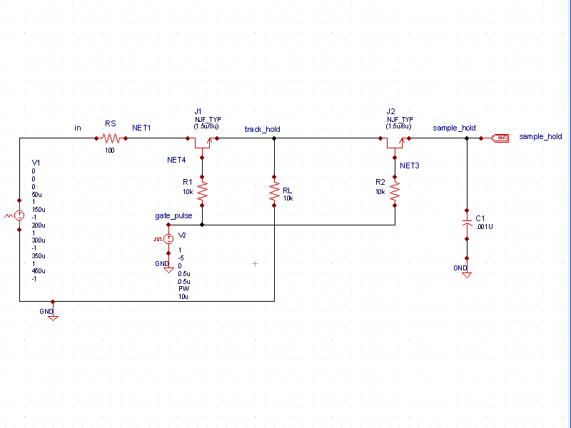
The schematic of the JFET sampling gate (see schematic.png ) shows the J1 JFET device used as a switch to sample the instantaneous amplitude of the input signal V1 several times during each cycle of the signal. J1 is switched on and off by the control voltage V2 applied to the gate terminal of the JFET. The addition of the capacitor C1 provides the abillity to hold the output voltage constant until the next sampling instant.
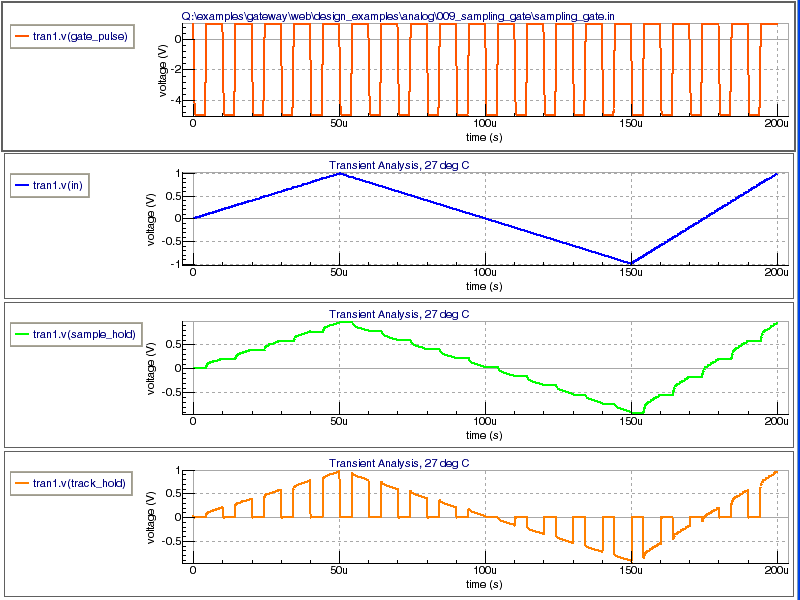
Simulating the example and then splitting the waveforms.png on separate charts shows the sample and hold functions
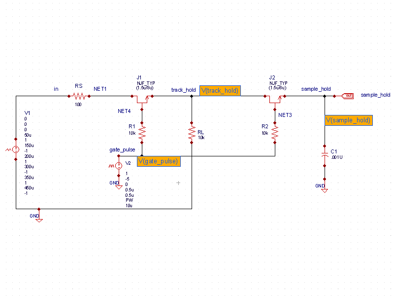
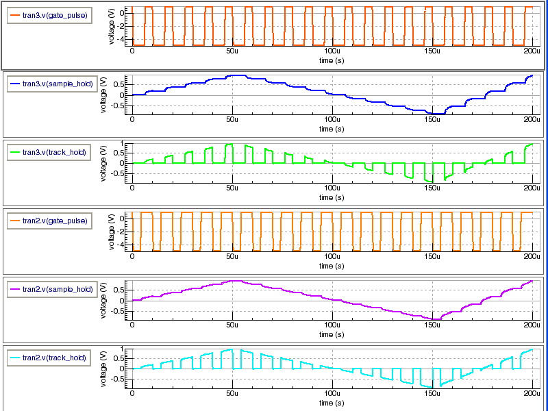
The control file for this example (see sampling_gate.ctr)shows a commented out .ST analysis that varies the pulse width of the sampling frequency. To enable the .ST, remove the asterisk character on the beginning of the line and save the control file. Then, on the schematic, switch to simulation mode (see simulation_mode.png ) and remove the input marker by clicking on the 'in' node. Re-simulating the design shows the results of the wider pulse width in the resulting waveforms (see ST_waveforms.png ).
sampling_gate.ctr
											*
.tran 5n 200u
.PARAM PW=3.5u
*.ST LIN PW 3.5u 6.5u 2u
***** MODELS *****
.MODEL NJF_TYP NJF      (VTO=-1.422 BETA=0.009109 LAMBDA=0.006 RD=1 RS=1
+ CGS=3.06E-13 CGD=4.57E-13 IS=2.052E-13 KF=1.23E-16 )
.model swmod SW VT=0.75v VH=0.01v RON=1 ROFF=1meg