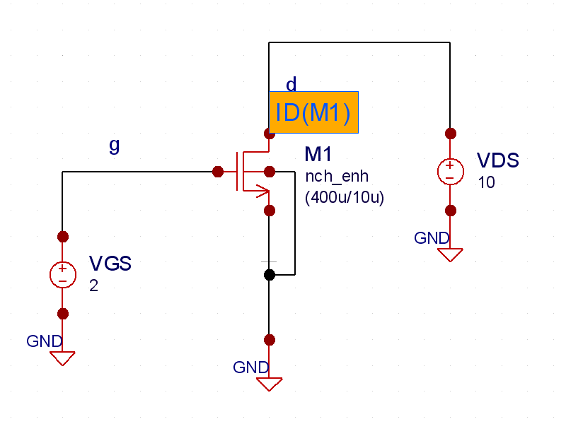
014_device_characterization : Nmos device characterization schematic
Minimum Required Versions: Gateway 2.12.8.R, SmartSpice 3.16.11.R
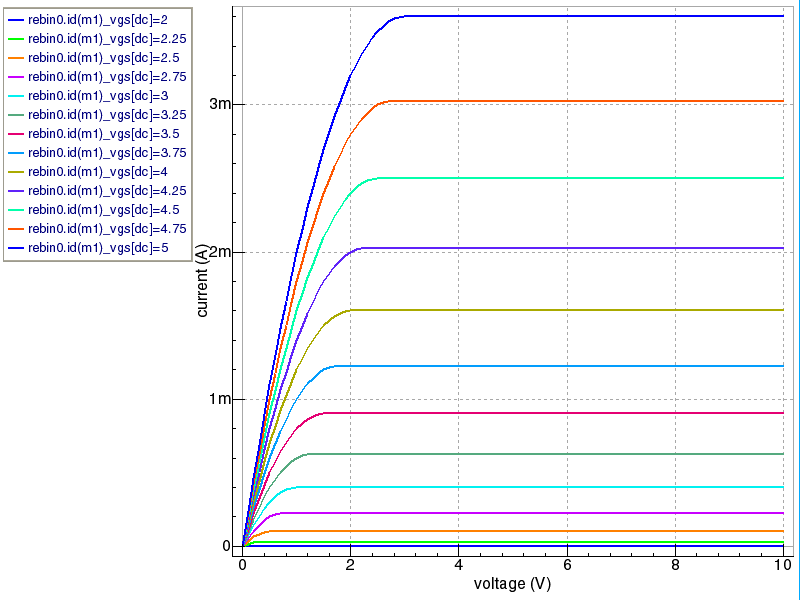
This example is a testbench schematic for testing MOS models and devices (see Example14.png ). In this example, a LEVEL=1 NMOS device is simulated, sweeping the drain-to-source voltage and the gate-to-source voltage. The .DC statement in the control file shows the syntax for the nested sweep. The resulting wave forms (see waveforms.png ) show the drain current versus drain-to-source voltage for the swept gate-to-source voltage levels between 2 and 5 volts.
Input Files
Graphics